MCHC908JW32FAE Freescale Semiconductor, MCHC908JW32FAE Datasheet - Page 95
MCHC908JW32FAE
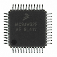
Manufacturer Part Number
MCHC908JW32FAE
Description
IC MCU 32K FLASH 8MHZ 48-LQFP
Manufacturer
Freescale Semiconductor
Series
HC08r
Datasheet
1.RD3152MMA7260Q.pdf
(232 pages)
Specifications of MCHC908JW32FAE
Core Processor
HC08
Core Size
8-Bit
Speed
8MHz
Connectivity
SPI, USB
Peripherals
LED, LVD, POR, PWM
Number Of I /o
29
Program Memory Size
32KB (32K x 8)
Program Memory Type
FLASH
Ram Size
1K x 8
Voltage - Supply (vcc/vdd)
3.5 V ~ 5.5 V
Oscillator Type
Internal
Operating Temperature
0°C ~ 70°C
Package / Case
48-LQFP
Controller Family/series
HC08
No. Of I/o's
48
Ram Memory Size
1KB
Cpu Speed
8MHz
No. Of Timers
1
Embedded Interface Type
SPI
Rohs Compliant
Yes
Processor Series
HC08JW
Core
HC08
Data Bus Width
8 bit
Data Ram Size
1 KB
Interface Type
SPI, USB
Number Of Programmable I/os
29
Number Of Timers
2
Maximum Operating Temperature
+ 70 C
Mounting Style
SMD/SMT
Development Tools By Supplier
FSICEBASE, DEMO908GZ60E, M68EML08GZE, KITUSBSPIDGLEVME, KITUSBSPIEVME, KIT33810EKEVME
Minimum Operating Temperature
0 C
Lead Free Status / RoHS Status
Lead free / RoHS Compliant
Eeprom Size
-
Data Converters
-
Lead Free Status / Rohs Status
Details
Available stocks
Company
Part Number
Manufacturer
Quantity
Price

Company:
Part Number:
MCHC908JW32FAE
Manufacturer:
Freescale Semiconductor
Quantity:
10 000
Part Number:
MCHC908JW32FAE
Manufacturer:
FREESCALE
Quantity:
20 000


7.3.1 Entering Monitor Mode
Table 7-1
may be entered after a POR and will allow communication at 9600 baud provided one of the following
sets of conditions is met:
If V
frequency is a divide-by-two of the input clock. If PTC1 is high with V
mode entry, the bus frequency will be a divide-by-four of the input clock. Holding the PTC1 pin low when
entering monitor mode causes a bypass of a divide-by-two stage at the oscillator only if V
to IRQ. In this event, the CGMOUT frequency is equal to the CGMXCLK frequency, and the OSC1 input
directly generates internal bus clocks. In this case, the OSC1 signal must have a 50% duty cycle at
maximum bus frequency.
The COP module is disabled in monitor mode as long as V
This condition states that as long as V
V
then the COP will be disabled. In the latter situation, after V
removed from the IRQ pin in the interest of freeing the IRQ for normal functionality in monitor mode.
Freescale Semiconductor
V
1. External clock is derived by a 4.9152/9.8304 MHz off-chip oscillator
2. Monitor mode entry by IRQ = V
V
GND
TST
IRQ
TST
V
(2)
TST
or
1. IRQ = V
2. IRQ = V
X
DD
TST
lator circuit is bypassed.
(2)
is applied to RST after the initial reset to get into monitor mode (when V
–
–
is applied to IRQ and PTC1 is low upon monitor mode entry (above condition set 1), the bus
GND
V
V
V
RST
V
V
V
or
TST
or
TST
or
TST
shows the pin conditions for entering monitor mode. As specified in the table, monitor mode
DD
DD
DD
The external clock is 4.9152 MHz with PTC1 low
The external clock is 9.8304 MHz with PTC1 high
TST
TST
PTA2
X
X
0
0
(PLL off):
(PLL off):
Table 7-1. Monitor Mode Signal Requirements and Options
PTA1
X
X
1
1
TST
PTA0
, a 4.9152/9.8304 MHz off-chip oscillator must be used. The MCU internal crystal oscil-
X
X
1
1
MC68HC908JW32 Data Sheet, Rev. 6
TST
PTC1
X
0
1
X
is maintained on the IRQ pin after entering monitor mode, or if
External
Clock
4.9152
9.8304
MHz
MHz
X
X
(1)
2.4576
2.4576
Freq.
MHz
MHz
Bus
—
0
TST
TST
is applied to either IRQ or RST.
is applied to the RST pin, V
OFF
OFF
OFF
PLL
X
TST
Disabled
Disabled
Disabled
Enabled
applied to IRQ upon monitor
COP
TST
Baud
9600
9600
Rate
was applied to IRQ),
—
0
Functional Description
No operation until
reset goes high
PTA1 and PTA2
voltages only
required if
IRQ = V
PTC1 determines
frequency divider
PTA1 and PTA2
voltages only
required if
IRQ = V
PTC1 determines
frequency divider
Enters user mode
TST
TST
Comment
is applied
TST
TST
can be
;
;
95
Related parts for MCHC908JW32FAE
Image
Part Number
Description
Manufacturer
Datasheet
Request
R

Part Number:
Description:
Manufacturer:
Freescale Semiconductor, Inc
Datasheet:
Part Number:
Description:
Manufacturer:
Freescale Semiconductor, Inc
Datasheet:
Part Number:
Description:
Manufacturer:
Freescale Semiconductor, Inc
Datasheet:
Part Number:
Description:
Manufacturer:
Freescale Semiconductor, Inc
Datasheet:
Part Number:
Description:
Manufacturer:
Freescale Semiconductor, Inc
Datasheet:
Part Number:
Description:
Manufacturer:
Freescale Semiconductor, Inc
Datasheet:
Part Number:
Description:
Manufacturer:
Freescale Semiconductor, Inc
Datasheet:
Part Number:
Description:
Manufacturer:
Freescale Semiconductor, Inc
Datasheet:
Part Number:
Description:
Manufacturer:
Freescale Semiconductor, Inc
Datasheet:
Part Number:
Description:
Manufacturer:
Freescale Semiconductor, Inc
Datasheet:
Part Number:
Description:
Manufacturer:
Freescale Semiconductor, Inc
Datasheet:
Part Number:
Description:
Manufacturer:
Freescale Semiconductor, Inc
Datasheet:
Part Number:
Description:
Manufacturer:
Freescale Semiconductor, Inc
Datasheet:
Part Number:
Description:
Manufacturer:
Freescale Semiconductor, Inc
Datasheet:
Part Number:
Description:
Manufacturer:
Freescale Semiconductor, Inc
Datasheet: