MCHC908JW32FAE Freescale Semiconductor, MCHC908JW32FAE Datasheet - Page 214
MCHC908JW32FAE
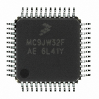
Manufacturer Part Number
MCHC908JW32FAE
Description
IC MCU 32K FLASH 8MHZ 48-LQFP
Manufacturer
Freescale Semiconductor
Series
HC08r
Datasheet
1.RD3152MMA7260Q.pdf
(232 pages)
Specifications of MCHC908JW32FAE
Core Processor
HC08
Core Size
8-Bit
Speed
8MHz
Connectivity
SPI, USB
Peripherals
LED, LVD, POR, PWM
Number Of I /o
29
Program Memory Size
32KB (32K x 8)
Program Memory Type
FLASH
Ram Size
1K x 8
Voltage - Supply (vcc/vdd)
3.5 V ~ 5.5 V
Oscillator Type
Internal
Operating Temperature
0°C ~ 70°C
Package / Case
48-LQFP
Controller Family/series
HC08
No. Of I/o's
48
Ram Memory Size
1KB
Cpu Speed
8MHz
No. Of Timers
1
Embedded Interface Type
SPI
Rohs Compliant
Yes
Processor Series
HC08JW
Core
HC08
Data Bus Width
8 bit
Data Ram Size
1 KB
Interface Type
SPI, USB
Number Of Programmable I/os
29
Number Of Timers
2
Maximum Operating Temperature
+ 70 C
Mounting Style
SMD/SMT
Development Tools By Supplier
FSICEBASE, DEMO908GZ60E, M68EML08GZE, KITUSBSPIDGLEVME, KITUSBSPIEVME, KIT33810EKEVME
Minimum Operating Temperature
0 C
Lead Free Status / RoHS Status
Lead free / RoHS Compliant
Eeprom Size
-
Data Converters
-
Lead Free Status / Rohs Status
Details
Available stocks
Company
Part Number
Manufacturer
Quantity
Price

Company:
Part Number:
MCHC908JW32FAE
Manufacturer:
Freescale Semiconductor
Quantity:
10 000
Part Number:
MCHC908JW32FAE
Manufacturer:
FREESCALE
Quantity:
20 000


Electrical Specifications
19.6 Control Timing
19.7 Internal RC Clock Timing
214
Pullup resistors
Low-voltage inhibit for external VDD, trip falling voltage
Low-voltage inhibit for external VDD, trip rising voltage
Internal operating frequency
RST input pulse width low
Internal RC Clock frequency
1. V
2. Typical values reflect average measurements at midpoint of voltage range, 25 °C only.
3. When V
4. Run (operating) I
5. Wait I
6. If minimum V
7. The internal 2.5V regulator has embedded a LVI_POR circuitry when the regulator voltage drops below V
8. R
9. The resistor value is measured at V
10. The resistor value is measured at V
1. V
2. Some modules may require a minimum frequency greater than dc for proper operation; see appropriate table for this
3. Minimum pulse width reset is guaranteed to be recognized. It is possible for a smaller pulse width to cause a reset.
1. V
PTA0–PTA7 configured as KBI0–KBI7
RST, IRQ, PTD2, PTD3, PTD7
PTE2–PTE3 with USB disabled
PTE2/D+ with USB enabled (to REG33V)
PTE3/D– with USB enabled (to REG33V)
PTB0–PTB7 with internal pullup enabled
(kick-in)
(recovery)
100 pF on all outputs. C
all outputs. C
V
voltage it triggers the CPU reset. The reset is released when the regulator voltage returns above V
information.
DD
SS
SS
DD
PU1
= 0 Vdc; timing shown with respect to 20% V
= 0 Vdc; timing shown with respect to 20% V
= 3.9 to 5.5 Vdc, V
is reached.
DD
and R
DD
measured using external square wave clock source. All inputs 0.2 V from rail. No dc loads. Less than 100 pF on
drops below 3.9V, the VREF33 regulator output will not be guaranteed within 3.3V +/- 10%.
PU2
(8)
DD
L
= 20 pF on OSC2. All ports configured as inputs. OSC2 capacitance linearly affects wait I
are measured at V
is not reached before the internal POR reset is released,
DD
Characteristic
Characteristic
Characteristic
measured using external square wave clock source. All inputs 0.2 V from rail. No dc loads. Less than
(3)
SS
L
Table 19-4. DC Electrical Characteristics (Continued)
(2)
= 20 pF on OSC2. All ports configured as inputs. OSC2 capacitance linearly affects run I
= 0 Vdc, T
(1)
DD
(1)
(1)
Table 19-6. Internal RC Clock Timing
DD
A
DD
= 5.0V
= T
= 3.9 to 5.5 Vdc, V
MC68HC908JW32 Data Sheet, Rev. 6
= 3.9 to 5.5 Vdc, V
(10)
(9)
Table 19-5. Control Timing
L
to T
H
, unless otherwise noted.
DD
DD
and 70% V
and 70% V
SS
R
SS
R
Symbol
V
PU4
V
= 0 Vdc.
PU4
R
R
R
R
TRIPR1
TRIPF1
= 0 Vdc.
PU1
PU2
PU3
PU5
Symbol
DD
Symbol
DD
(Tran)
(Idle)
f
f
t
, unless otherwise noted.
, unless otherwise noted.
OP
OP
RL
RST
1425
3.07
Min
must be driven low externally until minimum
900
Min
3.0
21
21
21
74
4
Min
100
—
Typ
TYP
88
3.3
3.4
30
30
30
—
—
5
(2)
Max
Freescale Semiconductor
—
8
LVI_POR_release
Max
105
1575
3090
Max
3.5
3.6
DD
39
39
39
6
.
LVI_POR_assert
MHz
Unit
voltage.
ns
Unit
DD
kHz
Unit
kΩ
kΩ
kΩ
kΩ
.
Ω
Ω
V
V
Related parts for MCHC908JW32FAE
Image
Part Number
Description
Manufacturer
Datasheet
Request
R

Part Number:
Description:
Manufacturer:
Freescale Semiconductor, Inc
Datasheet:
Part Number:
Description:
Manufacturer:
Freescale Semiconductor, Inc
Datasheet:
Part Number:
Description:
Manufacturer:
Freescale Semiconductor, Inc
Datasheet:
Part Number:
Description:
Manufacturer:
Freescale Semiconductor, Inc
Datasheet:
Part Number:
Description:
Manufacturer:
Freescale Semiconductor, Inc
Datasheet:
Part Number:
Description:
Manufacturer:
Freescale Semiconductor, Inc
Datasheet:
Part Number:
Description:
Manufacturer:
Freescale Semiconductor, Inc
Datasheet:
Part Number:
Description:
Manufacturer:
Freescale Semiconductor, Inc
Datasheet:
Part Number:
Description:
Manufacturer:
Freescale Semiconductor, Inc
Datasheet:
Part Number:
Description:
Manufacturer:
Freescale Semiconductor, Inc
Datasheet:
Part Number:
Description:
Manufacturer:
Freescale Semiconductor, Inc
Datasheet:
Part Number:
Description:
Manufacturer:
Freescale Semiconductor, Inc
Datasheet:
Part Number:
Description:
Manufacturer:
Freescale Semiconductor, Inc
Datasheet:
Part Number:
Description:
Manufacturer:
Freescale Semiconductor, Inc
Datasheet:
Part Number:
Description:
Manufacturer:
Freescale Semiconductor, Inc
Datasheet: