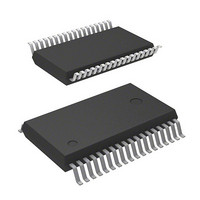
M37542F8FP#W4 Renesas Electronics America, M37542F8FP#W4 Datasheet - Page 101

M37542F8FP#W4
Manufacturer Part Number
M37542F8FP#W4
Description
IC 740 MCU FLASH 32K 36-SSOP
Manufacturer
Renesas Electronics America
Series
740/38000r
Datasheet
1.M37542F8FPU0.pdf
(124 pages)
Specifications of M37542F8FP#W4
Core Processor
740
Core Size
8-Bit
Speed
8MHz
Connectivity
SIO, UART/USART
Peripherals
POR, WDT
Number Of I /o
29
Program Memory Size
32KB (32K x 8)
Program Memory Type
FLASH
Ram Size
1K x 8
Voltage - Supply (vcc/vdd)
2.2 V ~ 5.5 V
Data Converters
A/D 8x10b
Oscillator Type
Internal
Operating Temperature
-20°C ~ 85°C
Package / Case
36-SSOP
Lead Free Status / RoHS Status
Lead free / RoHS Compliant
Eeprom Size
-
Available stocks
Company
Part Number
Manufacturer
Quantity
Price
7542 Group
Electrical Characteristics
Table 18 Electrical characteristics (1)
(FLASH ROM version: V
Notes 1: P1
Rev.3.03
REJ03B0006-0303
V
V
V
V
V
V
I
I
I
I
I
I
I
V
R
D
IH
IH
IH
IL
IL
IL
IL
Symbol
T+
T+
T+
OH
OL
OL
RAM
OSC
OSC
–V
–V
–V
2: R
3: It is available only when operating key-on wake up.
T–
T–
T–
X
1
D
“H” output voltage
P0
“L” output voltage
P0
P1
“L” output voltage
P0
Hysteresis
CNTR
P0
Hysteresis
R
Hysteresis
RESET
“H” input current
P0
“H” input current
RESET
“H” input current
X
“L” input current
P0
“L” input current
RESET
“L” input current
X
“L” input current
P0
RAM hold voltage
On-chip oscillator oscillation frequency
Oscillation stop detection circuit detection frequency
is measured when the P1
1
X
IN
IN
, S
Jul 11, 2008
0
0
0
0
0
D
0
0
0
–P0
–P0
–P1
–P0
–P0
–P0
–P0
–P0
CLK1
0
, S
0
, INT
7
7
4
7
7
7
7
7
CLK0
, INT
, P1
, P3
, P2
, P3
, P1
, P1
, P3
(Note 3)
0
0
, R
0
0
0
0
0
0
0
, INT
, and INT
–P1
–P3
–P2
–P3
–P1
–P1
–P3
CC
X
D
= 2.7 to 5.5V, Mask ROM version: V
4
7
7
7
4
4
7
1
1
, P2
, P2
, P2
, CAP
(Drive capacity = “L”)
(Drive capacity = “H”)
, S
Parameter
Page 99 of 117
1
CLK1
0
0
0
(P3
1
–P2
–P2
–P2
/T
0
, CAP
X
6
D
selected) have hysteresises only when bits 0 to 2 of the port P1P3 control register are set to “0” (CMOS level).
7
7
7
1
, P3
, P3
, P3
P-channel output disable bit of the UART1 control register (bit 4 of address 001B
1
0
0
0
(Note 2)
–P3
–P3
–P3
7
7
7
(Note 1)
I
V
I
Mask ROM: V
FLASH ROM: V
I
V
I
V
I
Mask ROM: V
FLASH ROM: V
I
V
I
V
I
Mask ROM: V
FLASH ROM: V
V
(Pin floating. Pull up transistors
“off”)
V
V
V
(Pin floating. Pull up transistors
“off”)
V
V
V
(Pull up transistors “on”)
When clock stopped
V
V
OH
OH
OL
OL
OL
OL
OL
OL
CC
CC
CC
CC
CC
I
I
I
I
I
I
I
CC
CC
CC
= V
= V
= V
= V
= V
= V
= V
= 5 mA
= 1.5 mA
= 1.0 mA
= 15 mA
= 1.5 mA
= 1.0 mA
= –5 mA
= –1.0 mA
= 4.0 to 5.5 V
= 4.0 to 5.5 V
= 4.0 to 5.5 V
= 4.0 to 5.5 V
= 4.0 to 5.5 V
= 5.0 V, Ta = 25 °C
= 5.0 V, Ta = 25 °C
= 2.2 to 5.5 V, V
CC
CC
CC
SS
SS
SS
SS
Test conditions
CC
CC
CC
CC
CC
CC
= 2.2 to 5.5 V
= 2.2 to 5.5 V
= 2.2 to 5.5 V
= 2.7 to 5.5 V
= 2.7 to 5.5 V
= 2.7 to 5.5 V
SS
= 0 V, Ta = –20 to 85 °C, unless otherwise noted)
V
V
CC
CC
1000
62.5
Min.
2.0
–1.5
–1.0
Limits
2000
–4.0
–0.2
Typ.
125
0.4
0.5
0.5
4.0
16
) is “0”.
187.5
3000
Max.
–5.0
–5.0
–0.5
1.5
0.3
1.0
2.0
0.3
1.0
5.0
5.0
5.5
Unit
kHz
kHz
mA
µA
µA
µA
µA
µA
µA
V
V
V
V
V
V
V
V
V
V
V
V


