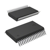
M37542F8FP#W4 Renesas Electronics America, M37542F8FP#W4 Datasheet - Page 70

M37542F8FP#W4
Manufacturer Part Number
M37542F8FP#W4
Description
IC 740 MCU FLASH 32K 36-SSOP
Manufacturer
Renesas Electronics America
Series
740/38000r
Datasheet
1.M37542F8FPU0.pdf
(124 pages)
Specifications of M37542F8FP#W4
Core Processor
740
Core Size
8-Bit
Speed
8MHz
Connectivity
SIO, UART/USART
Peripherals
POR, WDT
Number Of I /o
29
Program Memory Size
32KB (32K x 8)
Program Memory Type
FLASH
Ram Size
1K x 8
Voltage - Supply (vcc/vdd)
2.2 V ~ 5.5 V
Data Converters
A/D 8x10b
Oscillator Type
Internal
Operating Temperature
-20°C ~ 85°C
Package / Case
36-SSOP
Lead Free Status / RoHS Status
Lead free / RoHS Compliant
Eeprom Size
-
Available stocks
Company
Part Number
Manufacturer
Quantity
Price
NOTES ON PROGRAMMING
Processor Status Register
The contents of the processor status register (PS) after reset are
undefined except for the interrupt disable flag I which is “1”. After
reset, initialize flags which affect program execution. In particular,
it is essential to initialize the T flag and the D flag because of their
effect on calculations.
Interrupts
The contents of the interrupt request bit do not change even if the
BBC or BBS instruction is executed immediately after they are
changed by program because this instruction is executed for the
previous contents. For executing the instruction for the changed
contents, execute one instruction before executing the BBC or
BBS instruction.
Decimal Calculations
D to “1”, then execute the ADC instruction or SBC instruction. In
this case, execute SEC instruction, CLC instruction or CLD in-
struction after executing one instruction before the ADC instruction
or SBC instruction.
and Z (zero) flags are invalid.
Ports
That is, it is impossible to use the LDA instruction, memory opera-
tion instruction when the T flag is “1”, addressing mode using
direction register values as qualifiers, and bit test instructions such
as BBC and BBS.
It is also impossible to use bit operation instructions such as CLB
and SEB and read/modify/write instructions of direction registers
for calculations such as ROR.
For setting direction registers, use the LDM instruction, STA in-
struction, etc.
A/D Conversion
Do not execute the STP instruction during A/D conversion.
Instruction Execution Timing
The instruction execution time can be obtained by multiplying the
frequency of the internal clock φ by the number of cycles men-
tioned in the machine-language instruction table.
The frequency of the internal clock φ is the same as that of the X
in double-speed mode, twice the X
and 8 times the X
CPU Mode Register
The oscillation mode selection bit and processor mode bits can be
rewritten only once after releasing reset. However, after rewriting it
is disable to write any value to the bit. (Emulator MCU is ex-
cluded.)
When a ceramic oscillation is selected, a double-speed mode of
the clock division ratio selection bits can be used. Do not use it
when an RC oscillation is selected.
7542 Group
Rev.3.03
REJ03B0006-0303
• For calculations in decimal notation, set the decimal mode flag
• In the decimal mode, the values of the N (negative), V (overflow)
• The values of the port direction registers cannot be read.
Jul 11, 2008
IN
cycle in middle-speed mode.
Page 68 of 117
IN
cycle in high-speed mode
IN
State transition
Do not stop the clock selected as the operation clock because of
setting of CM3, 4.
NOTES ON HARDWARE
Handling of Power Source Pin
In order to avoid a latch-up occurrence, connect a capacitor suit-
able for high frequencies as bypass capacitor between power
source pin (Vcc pin) and GND pin (Vss pin). Besides, connect the
capacitor to as close as possible. For bypass capacitor which
should not be located too far from the pins to be connected, a ce-
ramic capacitor of 0.01 µF to 0.1 µF is recommended.
DATA REQUIRED FOR MASK ORDERS
The following are necessary when ordering a mask ROM produc-
tion:
1.Mask ROM Order Confirmation Form *
2.Mark Specification Form *
For the mask ROM confirmation and the mark specifications,
refer to the "Renesas Technology Corp." Homepage
(http://www.renesas.com/en/rom).


