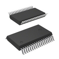
M37542F8FP#W4 Renesas Electronics America, M37542F8FP#W4 Datasheet - Page 30

M37542F8FP#W4
Manufacturer Part Number
M37542F8FP#W4
Description
IC 740 MCU FLASH 32K 36-SSOP
Manufacturer
Renesas Electronics America
Series
740/38000r
Datasheet
1.M37542F8FPU0.pdf
(124 pages)
Specifications of M37542F8FP#W4
Core Processor
740
Core Size
8-Bit
Speed
8MHz
Connectivity
SIO, UART/USART
Peripherals
POR, WDT
Number Of I /o
29
Program Memory Size
32KB (32K x 8)
Program Memory Type
FLASH
Ram Size
1K x 8
Voltage - Supply (vcc/vdd)
2.2 V ~ 5.5 V
Data Converters
A/D 8x10b
Oscillator Type
Internal
Operating Temperature
-20°C ~ 85°C
Package / Case
36-SSOP
Lead Free Status / RoHS Status
Lead free / RoHS Compliant
Eeprom Size
-
Available stocks
Company
Part Number
Manufacturer
Quantity
Price
7542 Group
• Interrupt Request Generation, Acceptance, and Handling
Interrupts have the following three phases.
(i) Interrupt Request Generation
(ii) Interrupt Request Acceptance
(iii) Handling of Accepted Interrupt Request
Figure 25 shows the time up to execution in the interrupt process-
ing routine, and Figure 26 shows the interrupt sequence.
Figure 27 shows the timing of interrupt request generation, inter-
rupt request bit, and interrupt request acceptance.
• Interrupt Handling Execution
When interrupt handling is executed, the following operations are
performed automatically.
(1) Once the currently executing instruction is completed, an in-
(2) The contents of the program counters and the processor sta-
(3) Concurrently with the push operation, the jump address of the
(4) The interrupt request bit for the corresponding interrupt is set
(5) The interrupt routine is executed.
(6) When the RTI instruction is executed, the contents of the reg-
As described above, it is necessary to set the stack pointer and
the jump address in the vector area corresponding to each inter-
rupt to execute the interrupt processing routine.
Rev.3.03
REJ03B0006-0303
An interrupt request is generated by an interrupt source (ex-
ternal interrupt signal input, timer underflow, etc.) and the
corresponding request bit is set to “1”.
Based on the interrupt acceptance timing in each instruction
cycle, the interrupt control circuit determines acceptance con-
ditions (interrupt request bit, interrupt enable bit, and interrupt
disable flag) and interrupt priority levels for accepting interrupt
requests. When two or more interrupt requests are generated
simultaneously, the highest priority interrupt is accepted. The
value of the interrupt request bit for an unaccepted interrupt
remains the same and acceptance is determined at the next
interrupt acceptance timing point.
The accepted interrupt request is processed.
terrupt request is accepted.
tus register at this point are pushed onto the stack area in
order from 1 to 3.
1.High-order bits of program counter (PCH)
2.Low-order bits of program counter (PCL)
3.Processor status register (PS)
corresponding interrupt (the start address of the interrupt pro-
cessing routine) is transferred from the interrupt vector to the
program counter.
to “0”. Also, the interrupt disable flag is set to “1” and multiple
interrupts are disabled.
isters pushed onto the stack area are popped off in the order
from 3 to 1. Then, the routine that was before running interrupt
processing resumes.
Jul 11, 2008
Page 28 of 117
When setting the followings, the interrupt request bit may be set to
“1”.
•When switching external interrupt active edge
Related registers:
Interrupt edge selection register (address 003A
Timer X mode register (address 002B
Capture mode register (address 0020
When not requiring the interrupt occurrence synchronized with
these setting, take the following sequence.
Fig. 25 Time up to execution in interrupt routine
Interrupt request
Notes on Interrupts
mode bit).
instructions have been executed.
Set the corresponding interrupt enable bit to “0” (disabled).
Set the interrupt edge select bit (active edge switch bit, trigger
Set the corresponding interrupt request bit to “0” after 1 or more
Set the corresponding interrupt enable bit to “1” (enabled).
generated
Main routine
* When executing DIV instruction
0 to 16* cycles
Interrupt request
acceptance
7 to 23 cycles
Interrupt sequence
Vector fetch
Stack push
7 cycles
16
16
)
)
Interrupt routine
starts
16
Interrupt handling
)
routine


