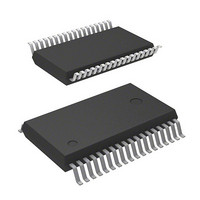
M37542F8FP#W4 Renesas Electronics America, M37542F8FP#W4 Datasheet - Page 87

M37542F8FP#W4
Manufacturer Part Number
M37542F8FP#W4
Description
IC 740 MCU FLASH 32K 36-SSOP
Manufacturer
Renesas Electronics America
Series
740/38000r
Datasheet
1.M37542F8FPU0.pdf
(124 pages)
Specifications of M37542F8FP#W4
Core Processor
740
Core Size
8-Bit
Speed
8MHz
Connectivity
SIO, UART/USART
Peripherals
POR, WDT
Number Of I /o
29
Program Memory Size
32KB (32K x 8)
Program Memory Type
FLASH
Ram Size
1K x 8
Voltage - Supply (vcc/vdd)
2.2 V ~ 5.5 V
Data Converters
A/D 8x10b
Oscillator Type
Internal
Operating Temperature
-20°C ~ 85°C
Package / Case
36-SSOP
Lead Free Status / RoHS Status
Lead free / RoHS Compliant
Eeprom Size
-
Available stocks
Company
Part Number
Manufacturer
Quantity
Price
7542 Group
The standard serial I/O mode inputs and outputs the software
commands, addresses and data needed to operate (read, pro-
gram, erase, etc.) the internal flash memory. This I/O is clock
synchronized serial. This mode requires a purpose-specific pe-
ripheral unit.
The standard serial I/O mode is different from the parallel I/O
mode in that the CPU controls flash memory rewrite (uses the
CPU rewrite mode), rewrite data input and so forth. The standard
serial I/O mode is started when the microcomputer is reset and
the CNV
high, P0
microcomputer mode, set CNVss pin to “L” level.)
This control program is written in the Boot ROM area when the
product is shipped from Renesas. Accordingly, make note of the
fact that the standard serial I/O mode cannot be used if the Boot
ROM area is rewritten in parallel I/O mode.
The standard serial I/O mode has standard serial I/O mode 1 of
the clock synchronous serial and the standard serial I/O mode 2 of
the clock asynchronous serial.
Table 13 lists the description of pin function (standard serial I/O
mode 1). Figures 107 to 109 show the pin connections for the
standard serial I/O mode 1.
Table 14 lists the description of pin function (standard serial I/O
mode 2). Figures 112 to 114 show the pin connections for the
standard serial I/O mode 2.
In standard serial I/O mode, only the User ROM area shown in
Figure 97 can be rewritten. The Boot ROM area cannot be written.
In standard serial I/O mode, a 7-byte ID code is used. When there
is data in the flash memory, this function determines whether the
ID code sent from the peripheral unit (programmer) and those writ-
ten in the flash memory match.The commands sent from the
peripheral unit (programmer) are not accepted unless the ID code
matches.
Rev.3.03
REJ03B0006-0303
Standard serial I/O Mode
SS
6
/S
pin high after pulling the P3
CLK2
Jul 11, 2008
pin low and P0
Page 85 of 117
5
/TxD
2
7
(RP) pin low, P3
pin high. (In the ordinary
2
(CE) pin


