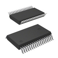
M37542F8FP#W4 Renesas Electronics America, M37542F8FP#W4 Datasheet - Page 88

M37542F8FP#W4
Manufacturer Part Number
M37542F8FP#W4
Description
IC 740 MCU FLASH 32K 36-SSOP
Manufacturer
Renesas Electronics America
Series
740/38000r
Datasheet
1.M37542F8FPU0.pdf
(124 pages)
Specifications of M37542F8FP#W4
Core Processor
740
Core Size
8-Bit
Speed
8MHz
Connectivity
SIO, UART/USART
Peripherals
POR, WDT
Number Of I /o
29
Program Memory Size
32KB (32K x 8)
Program Memory Type
FLASH
Ram Size
1K x 8
Voltage - Supply (vcc/vdd)
2.2 V ~ 5.5 V
Data Converters
A/D 8x10b
Oscillator Type
Internal
Operating Temperature
-20°C ~ 85°C
Package / Case
36-SSOP
Lead Free Status / RoHS Status
Lead free / RoHS Compliant
Eeprom Size
-
Available stocks
Company
Part Number
Manufacturer
Quantity
Price
7542 Group
(1) Standard serial I/O mode 1
Table 13 Description of pin function (standard serial I/O mode 1)
Rev.3.03
REJ03B0006-0303
V
CNV
RESET
X
X
V
P0
P0
P0
P0
P0
P1
P2
P3
P3
P3
CC
IN
OUT
REF
0
4
5
6
7
0
0
0
2
7
–P0
–P1
–P2
, P3
Pin name
,V
SS
SS
3
4
7
1
, P3
Jul 11, 2008
3
–P3
6
Power supply
CNV
Reset input
Clock input
Clock output
Reference voltage input
I/O port P0
RxD input
TxD output
S
BUSY output
I/O port P1
I/O port P2
I/O port P3
CE input
RP input
CLK
Signal name
SS
input
Page 86 of 117
I/O
I/O
I/O
I/O
I/O
O
O
O
I
I
I
I
I
I
I
I
I
Apply 2.7 to 5.5 V to the Vcc pin and 0 V to the Vss pin.
After input of port is set, input “H” level.
Reset input pin. System operates when RESET pin is set to “H” level after
CNVss pin is set to “H” level.
Connect an oscillation circuit between the X
As for the connection method, refer to the “clock generating circuit”.
(When system operates only by the on-chip oscillator, an external circuit is not
required.)
Apply reference voltage of A/D to this pin.
Input “L” or “H” level, or keep open.
Serial data input pin.
Serial data output pin.
Serial clock input pin.
BUSY signal output pin.
Input “L” or “H” level, or keep open.
Input “L” or “H” level, or keep open.
Input “L” or “H” level, or keep open.
Input “H” level.
Input “L” level.
Function
IN
and X
OUT
pins.


