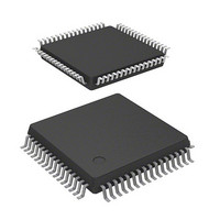
HD64F3672FPIV Renesas Electronics America, HD64F3672FPIV Datasheet - Page 234

HD64F3672FPIV
Manufacturer Part Number
HD64F3672FPIV
Description
MCU 3/5V 16K I-TEMP PB-FREE 64-L
Manufacturer
Renesas Electronics America
Series
H8® H8/300H Tinyr
Datasheet
1.HD64F3672FXV.pdf
(334 pages)
Specifications of HD64F3672FPIV
Core Processor
H8/300H
Core Size
16-Bit
Speed
16MHz
Connectivity
SCI
Peripherals
PWM, WDT
Number Of I /o
26
Program Memory Size
16KB (16K x 8)
Program Memory Type
FLASH
Ram Size
2K x 8
Voltage - Supply (vcc/vdd)
3 V ~ 5.5 V
Data Converters
A/D 4x10b
Oscillator Type
Internal
Operating Temperature
-40°C ~ 85°C
Package / Case
64-LQFP
For Use With
R0K436079S000BE - KIT DEV FOR H8/36079 W/COMPILER
Lead Free Status / RoHS Status
Lead free / RoHS Compliant
Eeprom Size
-
- Current page: 234 of 334
- Download datasheet (2Mb)
Section 14 A/D Converter
Legend:
14.3.3
ADCR enables A/D conversion started by an external trigger signal.
Rev.4.00 Nov. 02, 2005 Page 208 of 304
REJ09B0143-0400
Bit
2
1
0
Bit
7
6 to 1 —
0
Bit Name
CH2
CH1
CH0
Bit Name
TRGE
—
A/D Control Register (ADCR)
X: Don't care.
Initial Value
0
0
0
Initial Value
0
All 1
0
R/W
R/W
R/W
R/W
R/W
R/W
—
R/W
Description
Channel Select 0 to 2
Select analog input channels.
When SCAN = 0
X00: AN0
X01: AN1
X10: AN2
X11: AN3
Description
Trigger Enable
A/D conversion is started at the falling edge and the
rising edge of the external trigger signal (ADTRG)
when this bit is set to 1.
The selection between the falling edge and rising
edge of the external trigger pin (ADTRG) conforms
to the WPEG5 bit in the interrupt edge select
register 2 (IEGR2)
Reserved
These bits are always read as 1.
Reserved
Do not set this bit to 1, though the bit is
readable/writable.
When SCAN = 1
X00: AN0
X01: AN0 to AN1
X10: AN0 to AN2
X11: AN0 to AN3
Related parts for HD64F3672FPIV
Image
Part Number
Description
Manufacturer
Datasheet
Request
R

Part Number:
Description:
KIT STARTER FOR M16C/29
Manufacturer:
Renesas Electronics America
Datasheet:

Part Number:
Description:
KIT STARTER FOR R8C/2D
Manufacturer:
Renesas Electronics America
Datasheet:

Part Number:
Description:
R0K33062P STARTER KIT
Manufacturer:
Renesas Electronics America
Datasheet:

Part Number:
Description:
KIT STARTER FOR R8C/23 E8A
Manufacturer:
Renesas Electronics America
Datasheet:

Part Number:
Description:
KIT STARTER FOR R8C/25
Manufacturer:
Renesas Electronics America
Datasheet:

Part Number:
Description:
KIT STARTER H8S2456 SHARPE DSPLY
Manufacturer:
Renesas Electronics America
Datasheet:

Part Number:
Description:
KIT STARTER FOR R8C38C
Manufacturer:
Renesas Electronics America
Datasheet:

Part Number:
Description:
KIT STARTER FOR R8C35C
Manufacturer:
Renesas Electronics America
Datasheet:

Part Number:
Description:
KIT STARTER FOR R8CL3AC+LCD APPS
Manufacturer:
Renesas Electronics America
Datasheet:

Part Number:
Description:
KIT STARTER FOR RX610
Manufacturer:
Renesas Electronics America
Datasheet:

Part Number:
Description:
KIT STARTER FOR R32C/118
Manufacturer:
Renesas Electronics America
Datasheet:

Part Number:
Description:
KIT DEV RSK-R8C/26-29
Manufacturer:
Renesas Electronics America
Datasheet:

Part Number:
Description:
KIT STARTER FOR SH7124
Manufacturer:
Renesas Electronics America
Datasheet:

Part Number:
Description:
KIT STARTER FOR H8SX/1622
Manufacturer:
Renesas Electronics America
Datasheet:


