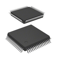
HD64F3672FPIV Renesas Electronics America, HD64F3672FPIV Datasheet - Page 325

HD64F3672FPIV
Manufacturer Part Number
HD64F3672FPIV
Description
MCU 3/5V 16K I-TEMP PB-FREE 64-L
Manufacturer
Renesas Electronics America
Series
H8® H8/300H Tinyr
Datasheet
1.HD64F3672FXV.pdf
(334 pages)
Specifications of HD64F3672FPIV
Core Processor
H8/300H
Core Size
16-Bit
Speed
16MHz
Connectivity
SCI
Peripherals
PWM, WDT
Number Of I /o
26
Program Memory Size
16KB (16K x 8)
Program Memory Type
FLASH
Ram Size
2K x 8
Voltage - Supply (vcc/vdd)
3 V ~ 5.5 V
Data Converters
A/D 4x10b
Oscillator Type
Internal
Operating Temperature
-40°C ~ 85°C
Package / Case
64-LQFP
For Use With
R0K436079S000BE - KIT DEV FOR H8/36079 W/COMPILER
Lead Free Status / RoHS Status
Lead free / RoHS Compliant
Eeprom Size
-
- Current page: 325 of 334
- Download datasheet (2Mb)
Item
Section 8 RAM
Section 10 Timer V
10.3.4 Timer
Control/Status Register V
(TCSRV)
Section 12 Watchdog
Timer
12.2.1 Timer
Control/Status Register
WD (TCSRWD)
Section 14 A/D Converter
14.3.1 A/D Data Registers
A to D (ADDRA to
ADDRD)
Section 17 Electrical
Characteristics
Table 17.2 DC
Characteristics (1)
Page
93
120
160
206
230
Revisions (See Manual for Details)
Note has been added.
Therefore byte access to ADDR should be done by reading
the upper byte first then the lower one. Word access is also
possible. ADDR is initialized to H'0000.
Bit
3
2
Bit
4
Item
Input high
voltage
Input low
voltage
Bit Name
OS3
OS2
Bit Name
TCSRWE
Symbol
V
V
IH
IL
Applicable
Pins
PB3 to PB0
RXD,
P12 to P10,
P17 to P14,
P22 to P20,
P57 to P50,
P76 to P74,
P84 to P80
PB3 to PB0
Description
Output Select 3 and 2
These bits select an output method
for the TMOV pin by the compare
match of TCORB and TCNTV.
00: No change
01: 0 output
10: 1 output
11: Output toggles
Description
Timer Control/Status Register WD
Write Enable
Rev.4.00 Nov. 02, 2005 Page 299 of 304
:
Test Condition
V
V
CC
CC
= 4.0 V to 5.5 V V
= 4.0 V to 5.5 V –0.3
REJ09B0143-0400
Values
Min
V
–0.3
CC
CC
0.7
0.8
Related parts for HD64F3672FPIV
Image
Part Number
Description
Manufacturer
Datasheet
Request
R

Part Number:
Description:
KIT STARTER FOR M16C/29
Manufacturer:
Renesas Electronics America
Datasheet:

Part Number:
Description:
KIT STARTER FOR R8C/2D
Manufacturer:
Renesas Electronics America
Datasheet:

Part Number:
Description:
R0K33062P STARTER KIT
Manufacturer:
Renesas Electronics America
Datasheet:

Part Number:
Description:
KIT STARTER FOR R8C/23 E8A
Manufacturer:
Renesas Electronics America
Datasheet:

Part Number:
Description:
KIT STARTER FOR R8C/25
Manufacturer:
Renesas Electronics America
Datasheet:

Part Number:
Description:
KIT STARTER H8S2456 SHARPE DSPLY
Manufacturer:
Renesas Electronics America
Datasheet:

Part Number:
Description:
KIT STARTER FOR R8C38C
Manufacturer:
Renesas Electronics America
Datasheet:

Part Number:
Description:
KIT STARTER FOR R8C35C
Manufacturer:
Renesas Electronics America
Datasheet:

Part Number:
Description:
KIT STARTER FOR R8CL3AC+LCD APPS
Manufacturer:
Renesas Electronics America
Datasheet:

Part Number:
Description:
KIT STARTER FOR RX610
Manufacturer:
Renesas Electronics America
Datasheet:

Part Number:
Description:
KIT STARTER FOR R32C/118
Manufacturer:
Renesas Electronics America
Datasheet:

Part Number:
Description:
KIT DEV RSK-R8C/26-29
Manufacturer:
Renesas Electronics America
Datasheet:

Part Number:
Description:
KIT STARTER FOR SH7124
Manufacturer:
Renesas Electronics America
Datasheet:

Part Number:
Description:
KIT STARTER FOR H8SX/1622
Manufacturer:
Renesas Electronics America
Datasheet:


