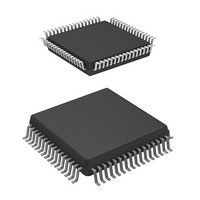
DF36034HJV Renesas Electronics America, DF36034HJV Datasheet - Page 432

DF36034HJV
Manufacturer Part Number
DF36034HJV
Description
MCU 3/5V 32K J-TEMP PB-FREE 64-Q
Manufacturer
Renesas Electronics America
Series
H8® H8/300H Tinyr
Specifications of DF36034HJV
Core Processor
H8/300H
Core Size
16-Bit
Speed
20MHz
Connectivity
CAN, SCI, SSU
Peripherals
PWM, WDT
Number Of I /o
45
Program Memory Size
32KB (32K x 8)
Program Memory Type
FLASH
Ram Size
2K x 8
Voltage - Supply (vcc/vdd)
3 V ~ 5.5 V
Data Converters
A/D 8x10b
Oscillator Type
Internal
Operating Temperature
-40°C ~ 85°C
Package / Case
64-QFP
For Use With
R0K436079S000BE - KIT DEV FOR H8/36079 W/COMPILER
Lead Free Status / RoHS Status
Lead free / RoHS Compliant
Eeprom Size
-
- Current page: 432 of 594
- Download datasheet (4Mb)
Section 18 A/D Converter
18.4.3
The A/D converter has a built-in sample-and-hold circuit. The A/D converter samples the analog
input when the A/D conversion start delay time (t
starts conversion. Figure 18.2 shows the A/D conversion timing. Table 18.3 shows the A/D
conversion time.
As indicated in figure 18.2, the A/D conversion time includes t
length of t
time therefore varies within the ranges indicated in table 18.3.
In scan mode, the values given in table 18.3 apply to the first conversion time. In the second and
subsequent conversions, the conversion time is 128 states (fixed) when CKS = 0 and 66 states
(fixed) when CKS = 1.
Rev. 4.00 Mar. 15, 2006 Page 398 of 556
REJ09B0026-0400
Input Sampling and A/D Conversion Time
D
varies depending on the timing of the write access to ADCSR. The total conversion
Address
Write signal
Input sampling
timing
ADF
[Legend]
(1):
(2):
t
t
t
D
SPL
CONV
:
:
:
ADCSR write cycle
ADCSR address
A/D conversion start delay time
Input sampling time
A/D conversion time
Figure 18.2 A/D Conversion Timing
(1)
(2)
t
D
t
SPL
D
) has passed after the ADST bit is set to 1, then
t
CONV
D
and the input sampling time. The
Related parts for DF36034HJV
Image
Part Number
Description
Manufacturer
Datasheet
Request
R

Part Number:
Description:
Headers & Wire Housings 20P PLUG METAL COVER
Manufacturer:
Hirose Electric Co Ltd

Part Number:
Description:
Headers & Wire Housings 25P PLUG METAL COVER
Manufacturer:
Hirose Electric Co Ltd

Part Number:
Description:
Headers & Wire Housings 15P PLUG METAL COVER
Manufacturer:
Hirose Electric Co Ltd

Part Number:
Description:
0.4 Mm Pitch, 1.5 Mm Mated Height, Board-to-fine Coaxial Cable Connectors
Manufacturer:
Hirose Electric
Datasheet:

Part Number:
Description:
CONN RECEPT 40POS 0.4MM SMD GOLD
Manufacturer:
Hirose Electric Co Ltd
Datasheet:

Part Number:
Description:
KIT STARTER FOR M16C/29
Manufacturer:
Renesas Electronics America
Datasheet:

Part Number:
Description:
KIT STARTER FOR R8C/2D
Manufacturer:
Renesas Electronics America
Datasheet:

Part Number:
Description:
R0K33062P STARTER KIT
Manufacturer:
Renesas Electronics America
Datasheet:

Part Number:
Description:
KIT STARTER FOR R8C/23 E8A
Manufacturer:
Renesas Electronics America
Datasheet:

Part Number:
Description:
KIT STARTER FOR R8C/25
Manufacturer:
Renesas Electronics America
Datasheet:

Part Number:
Description:
KIT STARTER H8S2456 SHARPE DSPLY
Manufacturer:
Renesas Electronics America
Datasheet:

Part Number:
Description:
KIT STARTER FOR R8C38C
Manufacturer:
Renesas Electronics America
Datasheet:

Part Number:
Description:
KIT STARTER FOR R8C35C
Manufacturer:
Renesas Electronics America
Datasheet:

Part Number:
Description:
KIT STARTER FOR R8CL3AC+LCD APPS
Manufacturer:
Renesas Electronics America
Datasheet:

Part Number:
Description:
KIT STARTER FOR RX610
Manufacturer:
Renesas Electronics America
Datasheet:


