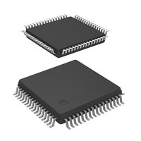
DF36037FZJV Renesas Electronics America, DF36037FZJV Datasheet - Page 430

DF36037FZJV
Manufacturer Part Number
DF36037FZJV
Description
MCU 3/5V 56K PB-FREE J-TEMP 64-L
Manufacturer
Renesas Electronics America
Series
H8® H8/300H Tinyr
Datasheet
1.DF36057GFZV.pdf
(594 pages)
Specifications of DF36037FZJV
Core Processor
H8/300H
Core Size
16-Bit
Speed
20MHz
Connectivity
CAN, SCI, SSU
Peripherals
PWM, WDT
Number Of I /o
45
Program Memory Size
56KB (56K x 8)
Program Memory Type
FLASH
Ram Size
3K x 8
Voltage - Supply (vcc/vdd)
3 V ~ 5.5 V
Data Converters
A/D 8x10b
Oscillator Type
Internal
Operating Temperature
-40°C ~ 85°C
Package / Case
64-LQFP
For Use With
R0K436079S000BE - KIT DEV FOR H8/36079 W/COMPILER
Lead Free Status / RoHS Status
Lead free / RoHS Compliant
Eeprom Size
-
- Current page: 430 of 594
- Download datasheet (4Mb)
Section 18 A/D Converter
18.3.3
ADCR enables A/D conversion started by an external trigger signal.
Rev. 4.00 Mar. 15, 2006 Page 396 of 556
REJ09B0026-0400
Bit
2
1
0
Bit
7
6 to 1
0
Bit Name
CH2
CH1
CH0
Bit Name
TRGE
—
—
A/D Control Register (ADCR)
Initial
Value
0
0
0
Initial
Value
0
All 1
0
R/W
R/W
R/W
R/W
R/W
R/W
—
R/W
Description
Channel Select 2 to 0
Select analog input channels.
When SCAN = 0
000: AN0
001: AN1
010: AN2
011: AN3
100: AN4
101: AN5
110: AN6
111: AN7
Description
Trigger Enable
A/D conversion is started at the falling edge and the rising
edge of the external trigger signal (ADTRG) when this bit
is set to 1.
The selection between the falling edge and rising edge of
the external trigger pin (ADTRG) conforms to the WPEG5
bit in the interrupt edge select register 2 (IEGR2)
Reserved
These bits are always read as 1.
Reserved
Although this bit is readable/writable, do not set this bit to
1.
When SCAN = 1
000: AN0
001: AN0 and AN1
010: AN0 to AN2
011: AN0 to AN3
100: AN4
101: AN4 and AN5
110: AN4 to AN6
111: AN4 to AN7
Related parts for DF36037FZJV
Image
Part Number
Description
Manufacturer
Datasheet
Request
R

Part Number:
Description:
Headers & Wire Housings 20P PLUG METAL COVER
Manufacturer:
Hirose Electric Co Ltd

Part Number:
Description:
Headers & Wire Housings 25P PLUG METAL COVER
Manufacturer:
Hirose Electric Co Ltd

Part Number:
Description:
Headers & Wire Housings 15P PLUG METAL COVER
Manufacturer:
Hirose Electric Co Ltd

Part Number:
Description:
0.4 Mm Pitch, 1.5 Mm Mated Height, Board-to-fine Coaxial Cable Connectors
Manufacturer:
Hirose Electric
Datasheet:

Part Number:
Description:
CONN RECEPT 40POS 0.4MM SMD GOLD
Manufacturer:
Hirose Electric Co Ltd
Datasheet:

Part Number:
Description:
KIT STARTER FOR M16C/29
Manufacturer:
Renesas Electronics America
Datasheet:

Part Number:
Description:
KIT STARTER FOR R8C/2D
Manufacturer:
Renesas Electronics America
Datasheet:

Part Number:
Description:
R0K33062P STARTER KIT
Manufacturer:
Renesas Electronics America
Datasheet:

Part Number:
Description:
KIT STARTER FOR R8C/23 E8A
Manufacturer:
Renesas Electronics America
Datasheet:

Part Number:
Description:
KIT STARTER FOR R8C/25
Manufacturer:
Renesas Electronics America
Datasheet:

Part Number:
Description:
KIT STARTER H8S2456 SHARPE DSPLY
Manufacturer:
Renesas Electronics America
Datasheet:

Part Number:
Description:
KIT STARTER FOR R8C38C
Manufacturer:
Renesas Electronics America
Datasheet:

Part Number:
Description:
KIT STARTER FOR R8C35C
Manufacturer:
Renesas Electronics America
Datasheet:

Part Number:
Description:
KIT STARTER FOR R8CL3AC+LCD APPS
Manufacturer:
Renesas Electronics America
Datasheet:

Part Number:
Description:
KIT STARTER FOR RX610
Manufacturer:
Renesas Electronics America
Datasheet:


