MC68HC908GP32CP Freescale Semiconductor, MC68HC908GP32CP Datasheet - Page 126
MC68HC908GP32CP
Manufacturer Part Number
MC68HC908GP32CP
Description
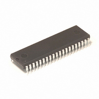
IC MCU 8MHZ 32K FLASH 40-DIP
Manufacturer
Freescale Semiconductor
Series
HC08r
Datasheet
1.MC68HC908GP32CFB.pdf
(410 pages)
Specifications of MC68HC908GP32CP
Core Processor
HC08
Core Size
8-Bit
Speed
8MHz
Connectivity
SCI, SPI
Peripherals
LVD, POR, PWM
Number Of I /o
33
Program Memory Size
32KB (32K x 8)
Program Memory Type
FLASH
Ram Size
512 x 8
Voltage - Supply (vcc/vdd)
2.7 V ~ 5.5 V
Data Converters
A/D 8x8b
Oscillator Type
Internal
Operating Temperature
-40°C ~ 85°C
Package / Case
40-DIP (0.600", 15.24mm)
For Use With
M68EVB908GP32 - BOARD EVALUATION FOR HC908GP32
Lead Free Status / RoHS Status
Contains lead / RoHS non-compliant
Eeprom Size
-
Available stocks
Company
Part Number
Manufacturer
Quantity
Price
Company:

Part Number:
MC68HC908GP32CP
Manufacturer:
ROCKWELL
Quantity:
201
Part Number:
MC68HC908GP32CP
Manufacturer:
MOTOROLA/摩托罗拉
Quantity:
20 000


Clock Generator Module (CGMC)
Technical Data
124
NOTE:
NOTE:
PLLON — PLL On Bit
BCS — Base Clock Select Bit
PLLON and BCS have built-in protection that prevents the base clock
selector circuit from selecting the VCO clock as the source of the base
clock if the PLL is off. Therefore, PLLON cannot be cleared when BCS
is set, and BCS cannot be set when PLLON is clear. If the PLL is off
(PLLON = 0), selecting CGMVCLK requires two writes to the PLL control
register. (See
PRE1 and PRE0 — Prescaler Program Bits
The value of P is normally 0 when using a 32.768-kHz crystal as the
reference.
This read/write bit activates the PLL and enables the VCO clock,
CGMVCLK. PLLON cannot be cleared if the VCO clock is driving the
base clock, CGMOUT (BCS = 1). (See
Circuit.) Reset sets this bit so that the loop can stabilize as the MCU
is powering up.
This read/write bit selects either the crystal oscillator output,
CGMXCLK, or the VCO clock, CGMVCLK, as the source of the
CGMC output, CGMOUT. CGMOUT frequency is one-half the
frequency of the selected clock. BCS cannot be set while the PLLON
bit is clear. After toggling BCS, it may take up to three CGMXCLK and
three CGMVCLK cycles to complete the transition from one source
clock to the other. During the transition, CGMOUT is held in stasis.
(See
These read/write bits control a prescaler that selects the prescaler
power-of-two multiplier, P. (See
Programming the
the PLLON bit is set. Reset clears these bits.
1 = PLL on
0 = PLL off
1 = CGMVCLK divided by two drives CGMOUT
0 = CGMXCLK divided by two drives CGMOUT
7.4.8 Base Clock Selector
Clock Generator Module (CGMC)
7.4.8 Base Clock Selector
PLL.) PRE1 and PRE0 cannot be written when
MC68HC908GP32
7.4.3 PLL Circuits
Circuit.) Reset clears the BCS bit.
7.4.8 Base Clock Selector
Circuit.)
•
MC68HC08GP32
and
7.4.6
MOTOROLA
—
Rev. 6
Related parts for MC68HC908GP32CP
Image
Part Number
Description
Manufacturer
Datasheet
Request
R

Part Number:
Description:
Manufacturer:
Freescale Semiconductor, Inc
Datasheet:
Part Number:
Description:
Manufacturer:
Freescale Semiconductor, Inc
Datasheet:
Part Number:
Description:
Manufacturer:
Freescale Semiconductor, Inc
Datasheet:
Part Number:
Description:
Manufacturer:
Freescale Semiconductor, Inc
Datasheet:
Part Number:
Description:
Manufacturer:
Freescale Semiconductor, Inc
Datasheet:
Part Number:
Description:
Manufacturer:
Freescale Semiconductor, Inc
Datasheet:
Part Number:
Description:
Manufacturer:
Freescale Semiconductor, Inc
Datasheet:
Part Number:
Description:
Manufacturer:
Freescale Semiconductor, Inc
Datasheet:
Part Number:
Description:
Manufacturer:
Freescale Semiconductor, Inc
Datasheet:
Part Number:
Description:
Manufacturer:
Freescale Semiconductor, Inc
Datasheet:
Part Number:
Description:
Manufacturer:
Freescale Semiconductor, Inc
Datasheet:
Part Number:
Description:
Manufacturer:
Freescale Semiconductor, Inc
Datasheet:
Part Number:
Description:
Manufacturer:
Freescale Semiconductor, Inc
Datasheet:
Part Number:
Description:
Manufacturer:
Freescale Semiconductor, Inc
Datasheet:
Part Number:
Description:
Manufacturer:
Freescale Semiconductor, Inc
Datasheet: