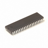
MC68HC908GP32CP Freescale Semiconductor, MC68HC908GP32CP Datasheet - Page 168

MC68HC908GP32CP
Manufacturer Part Number
MC68HC908GP32CP
Description
IC MCU 8MHZ 32K FLASH 40-DIP
Manufacturer
Freescale Semiconductor
Series
HC08r
Datasheet
1.MC68HC908GP32CFB.pdf
(410 pages)
Specifications of MC68HC908GP32CP
Core Processor
HC08
Core Size
8-Bit
Speed
8MHz
Connectivity
SCI, SPI
Peripherals
LVD, POR, PWM
Number Of I /o
33
Program Memory Size
32KB (32K x 8)
Program Memory Type
FLASH
Ram Size
512 x 8
Voltage - Supply (vcc/vdd)
2.7 V ~ 5.5 V
Data Converters
A/D 8x8b
Oscillator Type
Internal
Operating Temperature
-40°C ~ 85°C
Package / Case
40-DIP (0.600", 15.24mm)
For Use With
M68EVB908GP32 - BOARD EVALUATION FOR HC908GP32
Lead Free Status / RoHS Status
Contains lead / RoHS non-compliant
Eeprom Size
-
Available stocks
Company
Part Number
Manufacturer
Quantity
Price
Company:
Part Number:
MC68HC908GP32CP
Manufacturer:
ROCKWELL
Quantity:
201
Part Number:
MC68HC908GP32CP
Manufacturer:
MOTOROLA/摩托罗拉
Quantity:
20 000
- Current page: 168 of 410
- Download datasheet (3Mb)
FLASH Memory
11.4 FLASH Control Register
Technical Data
166
NOTE:
Address:
page. Hence the minimum erase page size is 128 bytes. Program and
erase operation operations are facilitated through control bits in FLASH
Control Register (FLCR). Details for these operations appear later in this
section. The address ranges for the user memory and vectors are:
Programming tools are available from Motorola. Contact your local
Motorola representative for more information.
A security feature prevents viewing of the FLASH contents.
The FLASH control register (FLCR) controls FLASH program and erase
operations.
HVEN — High-Voltage Enable Bit
1. No security feature is absolutely secure. However, Motorola’s strategy is to make reading or
copying the FLASH difficult for unauthorized users.
Reset:
Read:
Write:
•
•
•
•
This read/write bit enables the charge pump to drive high voltages for
program and erase operations in the array. HVEN can only be set if
either PGM = 1 or ERASE = 1 and the proper sequence for program
or erase is followed.
1 = High voltage enabled to array and charge pump on
0 = High voltage disabled to array and charge pump off
$8000–$FDFF; user memory.
$FF7E; FLASH block protect register.
$FE08
$FFDC–$FFFF; these locations are reserved for user-defined
interrupt and reset vectors.
$FE08
Bit 7
0
0
Figure 11-1. FLASH Control Register (FLCR)
;
FLASH control register.
FLASH Memory
6
0
0
5
0
0
MC68HC908GP32
4
0
0
HVEN
3
0
•
MASS
MC68HC08GP32
2
0
ERASE
1
0
1
MOTOROLA
—
PGM
Bit 0
Rev. 6
0
Related parts for MC68HC908GP32CP
Image
Part Number
Description
Manufacturer
Datasheet
Request
R
Part Number:
Description:
Manufacturer:
Freescale Semiconductor, Inc
Datasheet:
Part Number:
Description:
Manufacturer:
Freescale Semiconductor, Inc
Datasheet:
Part Number:
Description:
Manufacturer:
Freescale Semiconductor, Inc
Datasheet:
Part Number:
Description:
Manufacturer:
Freescale Semiconductor, Inc
Datasheet:
Part Number:
Description:
Manufacturer:
Freescale Semiconductor, Inc
Datasheet:
Part Number:
Description:
Manufacturer:
Freescale Semiconductor, Inc
Datasheet:
Part Number:
Description:
Manufacturer:
Freescale Semiconductor, Inc
Datasheet:
Part Number:
Description:
Manufacturer:
Freescale Semiconductor, Inc
Datasheet:
Part Number:
Description:
Manufacturer:
Freescale Semiconductor, Inc
Datasheet:
Part Number:
Description:
Manufacturer:
Freescale Semiconductor, Inc
Datasheet:
Part Number:
Description:
Manufacturer:
Freescale Semiconductor, Inc
Datasheet:
Part Number:
Description:
Manufacturer:
Freescale Semiconductor, Inc
Datasheet:
Part Number:
Description:
Manufacturer:
Freescale Semiconductor, Inc
Datasheet:
Part Number:
Description:
Manufacturer:
Freescale Semiconductor, Inc
Datasheet:
Part Number:
Description:
Manufacturer:
Freescale Semiconductor, Inc
Datasheet:


