CY8C3446LTI-073 Cypress Semiconductor Corp, CY8C3446LTI-073 Datasheet - Page 58
CY8C3446LTI-073
Manufacturer Part Number
CY8C3446LTI-073
Description
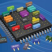
IC MCU 8BIT 64KB FLASH 48QFN
Manufacturer
Cypress Semiconductor Corp
Series
PSOC™ 3 CY8C34xxr
Specifications of CY8C3446LTI-073
Package / Case
*
Voltage - Supply (vcc/vdd)
1.71 V ~ 5.5 V
Operating Temperature
-40°C ~ 85°C
Speed
50MHz
Number Of I /o
25
Eeprom Size
2K x 8
Core Processor
8051
Program Memory Type
FLASH
Ram Size
8K x 8
Program Memory Size
64KB (64K x 8)
Data Converters
A/D 2x12b, D/A 2x8b
Oscillator Type
Internal
Peripherals
CapSense, DMA, POR, PWM, WDT
Connectivity
EBI/EMI, I²C, LIN, SPI, UART/USART, USB
Core Size
8-Bit
Operating Temperature (min)
-40C
Operating Temperature (max)
85C
Technology
CMOS
Processing Unit
Microcontroller
Operating Supply Voltage (min)
1.8V
Operating Supply Voltage (typ)
2.5/3.3/5V
Operating Supply Voltage (max)
5.5V
Package Type
QFN EP
Screening Level
Industrial
Pin Count
48
Mounting
Surface Mount
Rad Hardened
No
Processor Series
CY8C34
Core
8051
Data Bus Width
32 bit
Data Ram Size
8 KB
Interface Type
I2C, SPI, UART, USB
Maximum Clock Frequency
50 MHz
Number Of Programmable I/os
28 to 72
Number Of Timers
4
Operating Supply Voltage
1.71 V to 5.5 V
Maximum Operating Temperature
+ 85 C
Mounting Style
SMD/SMT
Controller Family/series
(8051) PSOC 3
No. Of I/o's
25
Eeprom Memory Size
2KB
Ram Memory Size
8KB
Cpu Speed
50MHz
Rohs Compliant
Yes
Lead Free Status / RoHS Status
Lead free / RoHS Compliant
Lead Free Status / RoHS Status
Compliant, Lead free / RoHS Compliant
Available stocks
Company
Part Number
Manufacturer
Quantity
Price

Part Number:
CY8C3446LTI-073
Manufacturer:
CYPRESS/赛普拉斯
Quantity:
20 000


The TIA configuration is used for applications where an external
sensor's output is current as a function of some type of stimulus
such as temperature, light, magnetic flux etc. In a common
application, the voltage DAC output can be connected to the
V
current by adjusting the voltage DAC output voltage.
8.6 LCD Direct Drive
The PSoC Liquid Crystal Display (LCD) driver system is a highly
configurable peripheral designed to allow PSoC to directly drive
a broad range of LCD glass. All voltages are generated on chip,
eliminating the need for external components. With a high
multiplex ratio of up to 1/16, the CY8C34 family LCD driver
system can drive a maximum of 736 segments. The PSoC LCD
driver module was also designed with the conservative power
budget of portable devices in mind, enabling different LCD drive
modes and power down modes to conserve power.
PSoC Creator provides an LCD segment drive component. The
component wizard provides easy and flexible configuration of
LCD resources. You can specify pins for segments and
commons along with other options. The software configures the
device to meet the required specifications. This is possible
because of the programmability inherent to PSoC devices.
Key features of the PSoC LCD segment system are:
Document Number: 001-53304 Rev. *K
REF
LCD panel direct driving
Type A (standard) and Type B (low-power) waveform support
Wide operating voltage range support (2 V to 5 V) for LCD
panels
Static, 1/2, 1/3, 1/4, 1/5 bias voltage levels
Internal bias voltage generation through internal resistor ladder
Up to 62 total common and segment outputs
Up to 1/16 multiplex for a maximum of 16 backplane/common
outputs
Up to 62 front plane/segment outputs for direct drive
Drives up to 736 total segments (16 backplane × 46 front plane)
Up to 64 levels of software controlled contrast
Ability to move display data from memory buffer to LCD driver
through DMA (without CPU intervention)
Adjustable LCD refresh rate from 10 Hz to 150 Hz
Ability to invert LCD display for negative image
Three LCD driver drive modes, allowing power optimization
TIA input to allow calibration of the external sensor bias
Figure 8-11. LCD System
8.6.1 LCD Segment Pin Driver
Each GPIO pin contains an LCD driver circuit. The LCD driver
buffers the appropriate output of the LCD DAC to directly drive
the glass of the LCD. A register setting determines whether the
pin is a common or segment. The pin’s LCD driver then selects
one of the six bias voltages to drive the I/O pin, as appropriate
for the display data.
8.6.2 Display Data Flow
The LCD segment driver system reads display data and
generates the proper output voltages to the LCD glass to
produce the desired image. Display data resides in a memory
buffer in the system SRAM. Each time you need to change the
common and segment driver voltages, the next set of pixel data
moves from the memory buffer into the Port Data Registers via
DMA.
8.6.3 UDB and LCD Segment Control
A UDB is configured to generate the global LCD control signals
and clocking. This set of signals is routed to each LCD pin driver
through a set of dedicated LCD global routing channels. In
addition to generating the global LCD control signals, the UDB
also produces a DMA request to initiate the transfer of the next
frame of LCD data.
8.6.4 LCD DAC
The LCD DAC generates the contrast control and bias voltage
for the LCD system. The LCD DAC produces up to five LCD drive
voltages plus ground, based on the selected bias ratio. The bias
voltages are driven out to GPIO pins on a dedicated LCD bias
bus, as required.
Global
Clock
DMA
UDB
Display
RAM
PSoC
PHUB
LCD Driver
Block
DAC
®
LCD
3: CY8C34 Family
Data Sheet
Page 58 of 126
PIN
[+] Feedback
Related parts for CY8C3446LTI-073
Image
Part Number
Description
Manufacturer
Datasheet
Request
R


Part Number:
Description:
Manufacturer:
Cypress Semiconductor Corp
Datasheet:
Part Number:
Description:
Manufacturer:
Cypress Semiconductor Corp
Datasheet:
Part Number:
Description:
Manufacturer:
Cypress Semiconductor Corp
Datasheet:
Part Number:
Description:
Manufacturer:
Cypress Semiconductor Corp
Datasheet:
Part Number:
Description:
Manufacturer:
Cypress Semiconductor Corp
Datasheet: