CY8C3446LTI-073 Cypress Semiconductor Corp, CY8C3446LTI-073 Datasheet - Page 83
CY8C3446LTI-073
Manufacturer Part Number
CY8C3446LTI-073
Description
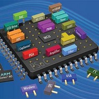
IC MCU 8BIT 64KB FLASH 48QFN
Manufacturer
Cypress Semiconductor Corp
Series
PSOC™ 3 CY8C34xxr
Specifications of CY8C3446LTI-073
Package / Case
*
Voltage - Supply (vcc/vdd)
1.71 V ~ 5.5 V
Operating Temperature
-40°C ~ 85°C
Speed
50MHz
Number Of I /o
25
Eeprom Size
2K x 8
Core Processor
8051
Program Memory Type
FLASH
Ram Size
8K x 8
Program Memory Size
64KB (64K x 8)
Data Converters
A/D 2x12b, D/A 2x8b
Oscillator Type
Internal
Peripherals
CapSense, DMA, POR, PWM, WDT
Connectivity
EBI/EMI, I²C, LIN, SPI, UART/USART, USB
Core Size
8-Bit
Operating Temperature (min)
-40C
Operating Temperature (max)
85C
Technology
CMOS
Processing Unit
Microcontroller
Operating Supply Voltage (min)
1.8V
Operating Supply Voltage (typ)
2.5/3.3/5V
Operating Supply Voltage (max)
5.5V
Package Type
QFN EP
Screening Level
Industrial
Pin Count
48
Mounting
Surface Mount
Rad Hardened
No
Processor Series
CY8C34
Core
8051
Data Bus Width
32 bit
Data Ram Size
8 KB
Interface Type
I2C, SPI, UART, USB
Maximum Clock Frequency
50 MHz
Number Of Programmable I/os
28 to 72
Number Of Timers
4
Operating Supply Voltage
1.71 V to 5.5 V
Maximum Operating Temperature
+ 85 C
Mounting Style
SMD/SMT
Controller Family/series
(8051) PSOC 3
No. Of I/o's
25
Eeprom Memory Size
2KB
Ram Memory Size
8KB
Cpu Speed
50MHz
Rohs Compliant
Yes
Lead Free Status / RoHS Status
Lead free / RoHS Compliant
Lead Free Status / RoHS Status
Compliant, Lead free / RoHS Compliant
Available stocks
Company
Part Number
Manufacturer
Quantity
Price

Part Number:
CY8C3446LTI-073
Manufacturer:
CYPRESS/赛普拉斯
Quantity:
20 000


11.2.2 Delta-sigma ADC
Unless otherwise specified, operating conditions are:
Table 11-20. 12-bit Delta-sigma ADC DC Specifications
Document Number: 001-53304 Rev. *K
Ge
Gd
Vos
TCVos
INL12
DNL12
INL8
DNL8
Rin_Buff
Rin_ADC12 ADC input resistance
Vextref
Current Consumption
I
I
Notes
Parameter
DD_12
BUFF
36. Based on device characterization (Not production tested).
37. By using switched capacitors at the ADC input an effective input resistance is created. Holding the gain and number of bits constant, the resistance is proportional
Operation in continuous sample mode
fclk = 6.144 MHz
Reference = 1.024 V internal reference bypassed on P3.2 or P0.3
Unless otherwise specified, all charts and graphs show typical values
to the inverse of the clock frequency. This value is calculated, not measured. For more information see the Technical Reference Manual.
Resolution
Number of channels, single ended
Number of channels, differential
Monotonic
Gain error
Gain drift
Input offset voltage
Temperature coefficient, input offset voltage
Input voltage range, single ended
Input voltage range, differential unbuffered
Input voltage range, differential, buffered
Integral non linearity
Differential non linearity
Integral non linearity
Differential non linearity
ADC input resistance
ADC external reference input voltage, see
also internal reference in
on page 85
Current consumption, 12 bit
Buffer current consumption
Description
[36]
[36]
[36]
[36]
Voltage Reference
[36]
[36]
[36]
[36]
[36]
Differential pair is formed using a pair
of GPIOs.
Yes
Buffered, buffer gain = 1,
Range = ±1.024 V, 25 °C
Buffered, buffer gain = 1,
Range = ±1.024 V
Buffered, 16-bit mode, V
25 °C
Buffer gain = 1, 16-bit,
Range = ±1.024 V
Range = ±1.024 V, unbuffered
Range = ±1.024 V, unbuffered
Range = ±1.024 V, unbuffered
Range = ±1.024 V, unbuffered
Input buffer used
Input buffer bypassed, 12 bit, Range
= ±1.024 V
Pins P0[3], P3[2]
192 ksps, unbuffered
Conditions
DDA
= 2.7 V,
PSoC
V
V
V
®
Min
0.9
10
SSA
SSA
SSA
8
–
–
–
–
–
–
–
–
–
–
–
–
–
–
3: CY8C34 Family
148
Typ
–
–
–
–
–
–
–
–
–
–
–
–
–
–
–
–
–
–
–
[37]
Data Sheet
V
GPIO/2
No. of
No. of
DDA
GPIO
V
V
Page 83 of 126
Max
±0.2
±0.1
1.3
1.4
2.5
12
50
55
±1
±1
±1
±1
DDA
DDA
–
–
–
– 1
ppm/°
µV/°C
Units
LSB
LSB
LSB
LSB
MΩ
bits
mV
mA
mA
kΩ
%
C
V
V
V
V
–
–
–
[+] Feedback
Related parts for CY8C3446LTI-073
Image
Part Number
Description
Manufacturer
Datasheet
Request
R


Part Number:
Description:
Manufacturer:
Cypress Semiconductor Corp
Datasheet:
Part Number:
Description:
Manufacturer:
Cypress Semiconductor Corp
Datasheet:
Part Number:
Description:
Manufacturer:
Cypress Semiconductor Corp
Datasheet:
Part Number:
Description:
Manufacturer:
Cypress Semiconductor Corp
Datasheet:
Part Number:
Description:
Manufacturer:
Cypress Semiconductor Corp
Datasheet: