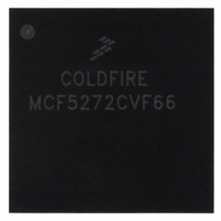
MCF5272CVF66 Freescale Semiconductor, MCF5272CVF66 Datasheet - Page 140

MCF5272CVF66
Manufacturer Part Number
MCF5272CVF66
Description
IC MPU 32BIT 66MHZ 196-MAPBGA
Manufacturer
Freescale Semiconductor
Series
MCF527xr
Specifications of MCF5272CVF66
Core Processor
Coldfire V2
Core Size
32-Bit
Speed
66MHz
Connectivity
EBI/EMI, Ethernet, I²C, SPI, UART/USART, USB
Peripherals
DMA, WDT
Number Of I /o
32
Program Memory Size
16KB (4K x 32)
Program Memory Type
ROM
Ram Size
1K x 32
Voltage - Supply (vcc/vdd)
3 V ~ 3.6 V
Oscillator Type
External
Operating Temperature
-40°C ~ 85°C
Package / Case
196-MAPBGA
Family Name
MCF5xxx
Device Core
ColdFire
Device Core Size
32b
Frequency (max)
66MHz
Instruction Set Architecture
RISC
Supply Voltage 1 (typ)
3.3V
Operating Temp Range
-40C to 85C
Operating Temperature Classification
Industrial
Mounting
Surface Mount
Pin Count
196
Package Type
MA-BGA
Lead Free Status / RoHS Status
Contains lead / RoHS non-compliant
Eeprom Size
-
Data Converters
-
Lead Free Status / Rohs Status
Not Compliant
Available stocks
Company
Part Number
Manufacturer
Quantity
Price
Company:
Part Number:
MCF5272CVF66
Manufacturer:
Freescale Semiconductor
Quantity:
10 000
Part Number:
MCF5272CVF66
Manufacturer:
FREESCALE
Quantity:
20 000
Company:
Part Number:
MCF5272CVF66 K75N
Manufacturer:
ST
Quantity:
18
Company:
Part Number:
MCF5272CVF66J
Manufacturer:
Freescale Semiconductor
Quantity:
10 000
- Current page: 140 of 544
- Download datasheet (7Mb)
Debug Support
5.5.3.3
The following sections describe the commands summarized in
Freescale reserves unassigned command opcodes for future expansion. Unused command formats in any
revision level perform a
5.5.3.3.1
Read the selected address or data register and return the 32-bit result. A bus error response is returned if
the CPU core is not halted.
Command/Result Formats:
Command Sequence:
Operand Data:
Result Data:
5-22
•
•
•
Command
Result
In cycle 3, the development system supplies the low-order 16 address bits. The debug module
always returns a not-ready response.
At the completion of cycle 3, the debug module initiates a memory read operation. Any serial
transfers that begin during a memory access return a not-ready response.
Results are returned in the two serial transfer cycles after the memory access completes. For any
command performing a byte-sized memory read operation, the upper 8 bits of the response data are
undefined and the referenced data is returned in the lower 8 bits. The next command’s opcode is
sent to the debug module during the final transfer. If a memory or register access is terminated with
a bus error, the error status (S = 1, DATA = 0x0001) is returned instead of result data.
Command Set Descriptions
The BDM status bit (S) is 0 for normally completed commands; S = 1 for
illegal commands, not-ready responses, and transfers with bus-errors.
Section 5.5.2, “BDM Serial
Read A/D Register (
15
MCF5272 ColdFire
None
The contents of the selected register are returned as a longword value,
most-significant word first.
0x2
NOP
Figure 5-18. RAREG
Figure 5-17. RAREG
and return an illegal command response.
RAREG/RDREG
12
???
RAREG
®
11
Integrated Microprocessor User’s Manual, Rev. 3
Interface,” describes the receive packet format.
/
0x1
RDREG
/
RDREG Command Sequence
NOTE
/
RDREG Command Format
MS RESULT
)
BERR
XXX
XXX
D[31:16]
8
D[15:0]
7
Table
LS RESULT
"NOT READY"
NEXT CMD
NEXT CMD
0x8
5-17.
4
A/D
3
Freescale Semiconductor
2
Register
0
Related parts for MCF5272CVF66
Image
Part Number
Description
Manufacturer
Datasheet
Request
R
Part Number:
Description:
Mcf5272 Coldfire Integrated Microprocessor User
Manufacturer:
Freescale Semiconductor, Inc
Datasheet:

Part Number:
Description:
MCF5272 Interrupt Service Routine for the Physical Layer Interface Controller
Manufacturer:
Freescale Semiconductor / Motorola
Datasheet:
Part Number:
Description:
Manufacturer:
Freescale Semiconductor, Inc
Datasheet:
Part Number:
Description:
Manufacturer:
Freescale Semiconductor, Inc
Datasheet:
Part Number:
Description:
Manufacturer:
Freescale Semiconductor, Inc
Datasheet:
Part Number:
Description:
Manufacturer:
Freescale Semiconductor, Inc
Datasheet:
Part Number:
Description:
Manufacturer:
Freescale Semiconductor, Inc
Datasheet:
Part Number:
Description:
Manufacturer:
Freescale Semiconductor, Inc
Datasheet:
Part Number:
Description:
Manufacturer:
Freescale Semiconductor, Inc
Datasheet:
Part Number:
Description:
Manufacturer:
Freescale Semiconductor, Inc
Datasheet:
Part Number:
Description:
Manufacturer:
Freescale Semiconductor, Inc
Datasheet:
Part Number:
Description:
Manufacturer:
Freescale Semiconductor, Inc
Datasheet:
Part Number:
Description:
Manufacturer:
Freescale Semiconductor, Inc
Datasheet:
Part Number:
Description:
Manufacturer:
Freescale Semiconductor, Inc
Datasheet:
Part Number:
Description:
Manufacturer:
Freescale Semiconductor, Inc
Datasheet:


