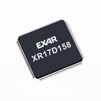
XR17D154IV-F Exar Corporation, XR17D154IV-F Datasheet - Page 12

XR17D154IV-F
Manufacturer Part Number
XR17D154IV-F
Description
IC UART PCI BUS QUAD 144LQFP
Manufacturer
Exar Corporation
Type
IrDA or RS- 485r
Datasheet
1.XR17D154CV-F.pdf
(69 pages)
Specifications of XR17D154IV-F
Number Of Channels
4, QUART
Package / Case
144-LQFP
Features
*
Fifo's
64 Byte
Protocol
RS485
Voltage - Supply
3.3V, 5V
With Auto Flow Control
Yes
With Irda Encoder/decoder
Yes
With False Start Bit Detection
Yes
With Modem Control
Yes
Mounting Type
Surface Mount
Data Rate
6.25 Mbps
Supply Voltage (max)
5.5 V
Supply Voltage (min)
3 V
Supply Current
4 mA
Maximum Operating Temperature
+ 85 C
Minimum Operating Temperature
- 40 C
Mounting Style
SMD/SMT
Operating Supply Voltage
3.3 V or 5 V
No. Of Channels
4
Uart Features
Tx/Rx FIFO Counters
Supply Voltage Range
3V To 5.5V
Operating Temperature Range
-40°C To +85°C
Digital Ic Case Style
LQFP
Rohs Compliant
Yes
Lead Free Status / RoHS Status
Lead free / RoHS Compliant
Lead Free Status / RoHS Status
Lead free / RoHS Compliant, Lead free / RoHS Compliant
Other names
1016-1290
Available stocks
Company
Part Number
Manufacturer
Quantity
Price
Company:
Part Number:
XR17D154IV-F
Manufacturer:
ADI
Quantity:
1 046
Company:
Part Number:
XR17D154IV-F
Manufacturer:
Exar Corporation
Quantity:
10 000
XR17D154
UNIVERSAL (3.3V AND 5V) PCI BUS QUAD UART
N
The device configuration registers and a special way to access each of the UART’s transmit and receive data
FIFOs are accessible directly from the PCI data bus. This provides easy programming of general operating
parameters to the D154 UART and for monitoring the status of various functions. The registers occupy 2K of
PCI bus memory address space. These addresses are offset onto the basic memory address, a value loaded
into the Memory Base Address Register (BAR) in the PCI local bus configuration register set. These registers
control or report on all 4 channel UARTs functions that include interrupt control and status, 16-bit general
purpose timer control and status, multipurpose inputs/outputs control and status, sleep mode control, soft-reset
control, and device identification and revision, and others.
The registers set is mapped into 4 address blocks where each UART channel occupies 512 bytes memory
space for its own 16550 compatible configuration registers. The device configuration and control registers are
embedded inside the UART channel zero’s address space between 0x0080 to 0x0093. All these registers can
be accessed in 8, 16, 24 or 32 bit width depending on the starting address given by the host at beginning of the
bus cycle. Transmit and receive data may be loaded or unloaded in 8, 16, 24 or 32 bit format to the register’s
address. Every time a read or write operation is made to the transmit or receive register, its FIFO data pointer
is automatically bumped to the next sequential data location either in byte, word or dword. One special case
applies to the receive data unloading when reading the receive data together with its LSR register content. The
host must read them in 16 or 32 bits format in order to maintain integrity of the data byte with its associated
error flags.
2.2
OTE
A
DDRESS
0x3C
0x30
0x34
0x38
: RWR
Device configuration Register Set
1
=Read/Write from external EEPROM. RWR=Read/Write from AD[31:0]. RO= Read Only. WO=Write Only.
15:0
31:0
31:0
31:0
31:24
23:16
15:8
7:0
B
ITS
RWR
RWR
T
RO
RO
RO
RO
RO
RO
T
YPE
ABLE
1
2: PCI L
Subsystem Vendor ID (write from external EEPROM by cus-
tomer)
Expansion ROM Base Address (Unimplemented)
Reserved (returns zeros)
Reserved (returns zeros)
Unimplemented MAXLAT
Unimplemented MINGNT
Interrupt Pin, use INTA#.
Interrupt Line.
OCAL
B
US
C
ONFIGURATION
12
D
ESCRIPTION
S
PACE
R
EGISTERS
xr
R
0x00000000
0x00000000
0x00000000
ESET
0x0000
(
0xXX
0x00
0x00
0x01
HEX
REV. 1.2.2
V
ALUE
)


