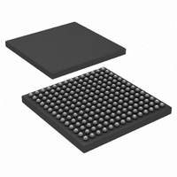
HSP50216KIZ Intersil, HSP50216KIZ Datasheet - Page 18

HSP50216KIZ
Manufacturer Part Number
HSP50216KIZ
Description
IC DOWNCONVERTER DGTL 4CH 196BGA
Manufacturer
Intersil
Datasheet
1.HSP50216KIZ.pdf
(58 pages)
Specifications of HSP50216KIZ
Function
Downconverter
Rf Type
W-CDMA
Package / Case
196-BGA
Lead Free Status / RoHS Status
Lead free / RoHS Compliant
POSITIONS
28:18
31:29
41:32
44:42
52:45
BIT
Block-to-Block Step
Round Select
Data Memory
Data Memory
Data Memory
FUNCTION
Destination
Block Start
Block Size
18
Destination Field Bit Mapping
31:29
28
AGCLFGN AGCLF
000
001
010
011
100
101
110
111
Provided for use with the coefficient down-shift bits.
Memory block base address, 0-1023, 0-383 are valid for the HSP50216.
44:42
0
1
2
3
4
5
6
7
(modulo addressing is used).
0-255, usually equal to the decimation factor for the FIR in this instruction.
AGCLFGNAGC loop gain select. Only applies to Path 1.
AGCLF
Path(1:0) Back End Data Routing Path Selection.
OS
FB
F(4:0)
INSTRUCTION BIT FIELDS (Continued)
AGC loop filter enable. Only applies to Path 1. The AGC loop is updated with the magnitude
00Route output back to filter compute engine input to another FIR in the filter chain.
01Route output through the FIFO and AGC forward path to the cartesian-to-polar coordinate
10Route output directly to the output, bypassing the FIFO and AGC (I2, Q2). This path also
Enable output strobe. Setting this bit generates a data ready signal when the data reaches
Feedback data path. When set, the magnitude and dphi/dt from the cartesian-to-polar coor-
Filter select. For data recirculated to the input of the FIR processor by path 0 or from the car-
Round Select (Add rounding bit at specified location).
2
2
2
2
2
2
2
no rounding.
Block Size.
8
16
32
64
128
256
512
1024
27
Loop gain 0 or 1 if AGCLF bit is set. Set to 0 (1 is a test mode for future chips).
of this sample (Path(1:0) = 01).
converter conversion and output (I1, Q1, magnitude, phase, gain) and also to route to a dis-
criminator (i.e., dφ/dt FIR).
routes to next channel FIR input.
the output section and starts the serial output sequence (paths 1, 2, 3). If OS is not set,
there will be no output to the outside world from this channel, for that output calculation, but
the data will be loaded into its output holding register (OS would not be set when routing the
data to another back end when cascading channels).
dinate converter block are routed to the filter compute engine input (magnitude goes to the
I input and dphi/dt goes to the Q input). Provided for discriminator filtering.
tesian to polar coordinate converter output, these bits tell which filter sequencer step gets it
as an input.
-24
-23
-22
-21
-20
-19
-18
, use this code when downshifting is not used.
HSP50216
26
Path1
25
Path0
24
OS
DESCRIPTION
23
FB
22
F4
21
F3
20
F2
19
F1
18
F0
August 17, 2007
FN4557.6


