HSP50216KIZ Intersil, HSP50216KIZ Datasheet - Page 30
HSP50216KIZ
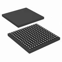
Manufacturer Part Number
HSP50216KIZ
Description
IC DOWNCONVERTER DGTL 4CH 196BGA
Manufacturer
Intersil
Datasheet
1.HSP50216KIZ.pdf
(58 pages)
Specifications of HSP50216KIZ
Function
Downconverter
Rf Type
W-CDMA
Package / Case
196-BGA
Lead Free Status / RoHS Status
Lead free / RoHS Compliant


μP Read/Write Procedures
To Write to the Internal Registers:
To Write to the Internal Instruction/Coefficient
RAMs:
To Read Internal Registers:
To Read Data Outputs:
To Read Instruction/Coefficient Values:
1. Load the indirect write holding registers at direct address
2. Write the Indirect Write Address of the internal register
3. Wait 4 clock cycles before performing the next write to the
1. Put the filter compute engine of the desired channel into
2. Load the indirect write holding registers at direct address
3. Write the Indirect Write Address of the internal RAM
4. Wait 4 clock cycles before performing the next write to the
5. After all data has been loaded, set the μPHold bit back
1. Write the Indirect Read Address of the internal register
2. Perform a read of the Indirect Read Holding Registers at
1. Set up the μP FIFO Read Order Control Register (located
2. Wait for interrupt or check flag.
3. Data can then be read, 16 bits at a time, at direct
4. Repeat step 3 for desired number of words.
5. Go to step 2.
1. Put the filter compute engine of the desired channel into
ADD(2:0) = 0 and 1 with the data for the internal register
(16 or 32 bits depending on the internal register being
addressed).
being addressed to direct address ADD(2:0) = 2 (Note: A
write strobe to transfer the contents of the Indirect Write
Holding Register into the Target Register specified by the
Indirect Address will be generated internally).
indirect write holding registers.
the hold mode by setting bit 31 of the Filter Compute
Engine / Resampler Control register located at
IWA = *00Ah (Note: The * is equal to 0, 1, 2 or 3
depending on the channel being addressed). By setting
bit 31 all FIR processing for the channel addressed will be
stopped.
ADD(2:0) = 0 and 1 with the data for the internal RAM
location.
location being addressed to direct address ADD(2:0) = 2
(Note: A write strobe to transfer the contents of the
Indirect Write Holding Register into the RAM location
specified by the Indirect Address will be generated
internally).
indirect write holding registers.
low.
being addressed to direct address ADD(2:0) = 3.
direct address ADD(2:0) = 0 and 1.
at Global Write Address (GWA) = F820h - F83Fh).
address 2, ADD(2:0) = 2.
the hold mode by setting bit 31 of the Filter Compute
Engine / Resampler Control register located at
30
HSP50216
Recommended HSP50216 configuration
procedure following a hardware reset (i.e.
RESETb is pulsed low):
NOTE: For the latter method, the SYNCO pin must be connected to
the SYNCI pin.
Recommended HSP50216 Channel
Reconfiguration Procedure:
NOTE: For the latter method, the SYNCO pin must be connected to
the SYNCI pin.
2. Write the Indirect Read Address (IRA) of the internal
3. Wait 4 clock cycles.
4. Read the data at direct address ADD(2:0) = 0 and 1.
5. After all the data has been read, set the μPHold bit back
1. Load Global Write Address registers GWA F800 - GWA
2. For each signal processing channel (0-3):
3. Generate a SYNCI to enable the input data or to
1. Disable the serial output for the desired channel in
2. Disable the interrupts from the channel in register GWA
3. Set the mPHold bit in register IWA *00A - 31 to give the
4. Load the new filter configuration.
5. Load any other channel registers.
6. Clear the mPHold bit in register IWA *00A - 31.
7. Do a software channel reset by writing to IWA *019.
8. Enable the serial outputs (GWA F801) and interrupts
9. Generate a SYNCI to enable the input data or to
IWA = *00Ah (Note: The * is equal to 0, 1, 2 or 3
depending on the channel being addressed).
RAM/ROM location being addressed to direct address
ADD(2:0) = 3.
low.
F808 and GWA F820 - GWA F83F.
a. Set mPHold bit located at Indirect Write Address
b. Load Filter Compute Engine Instruction RAMS.
c. Load Filter Compute Engine Coefficient RAMS.
d. Load IWA registers *000 - *019. (Clear the mPHold bit
e. Wait 32 clocks (CLK) for the reset to complete in the
register GWA F801 - 3, 2, 1 or 0.
F802 - 31, 23, 15, or 7.
processor access to the Filter Compute Engine
Instruction RAMS and Coefficient RAMS.
(GWA F802).
synchronize the processing to external events or
generate a SYNCO by writing to GWA F809.
synchronize the processing to external events or
generate a SYNCO by writing to GWA F809.
register IWA *00A - 31.
in register IWA *00A - 31).
Filter Compute Engine.
August 17, 2007
FN4557.6
Related parts for HSP50216KIZ
Image
Part Number
Description
Manufacturer
Datasheet
Request
R

Part Number:
Description:
Intersil Corporation [CMOS Serial Controller Interface]
Manufacturer:
Intersil Corporation
Datasheet:
Part Number:
Description:
Manufacturer:
Intersil Corporation
Datasheet:
Part Number:
Description:
357-036-542-201 CARDEDGE 36POS DL .156 BLK LOPRO
Manufacturer:
Intersil Corporation
Datasheet:
Part Number:
Description:
1024-Word x 4-Bit LSI Static RAM
Manufacturer:
Intersil Corporation
Datasheet:
Part Number:
Description:
General Purpose NPN Transistor Arrays FN341.4
Manufacturer:
Intersil Corporation
Datasheet:
Part Number:
Description:
CMOS 16-Bit Microprocessor
Manufacturer:
Intersil Corporation
Datasheet:
Part Number:
Description:
Manufacturer:
Intersil Corporation
Datasheet:
Part Number:
Description:
Manufacturer:
Intersil Corporation
Datasheet:
Part Number:
Description:
Manufacturer:
Intersil Corporation
Datasheet:
Part Number:
Description:
Manufacturer:
Intersil Corporation
Datasheet:
Part Number:
Description:
CMOS 6-Bit Latch and Decoder Memory Interfaces
Manufacturer:
Intersil Corporation
Datasheet:
Part Number:
Description:
CA3046General Purpose NPN Transistor Arrays
Manufacturer:
Intersil Corporation
Datasheet:
Part Number:
Description:
Manufacturer:
Intersil Corporation
Datasheet:
Part Number:
Description:
TR909 DLC/FLC SLIC with Low Power Standby
Manufacturer:
Intersil Corporation
Datasheet:
Part Number:
Description:
Manufacturer:
Intersil Corporation
Datasheet: