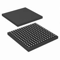
HSP50216KIZ Intersil, HSP50216KIZ Datasheet - Page 29

HSP50216KIZ
Manufacturer Part Number
HSP50216KIZ
Description
IC DOWNCONVERTER DGTL 4CH 196BGA
Manufacturer
Intersil
Datasheet
1.HSP50216KIZ.pdf
(58 pages)
Specifications of HSP50216KIZ
Function
Downconverter
Rf Type
W-CDMA
Package / Case
196-BGA
Lead Free Status / RoHS Status
Lead free / RoHS Compliant
Microprocessor Interface
Data reads can be direct, indirect or FIFO-like depending on
the data that is being read. The status register is read directly
at direct (external) address 3, ADD(2:0) = 3. Readback of
internal registers and memories is indirect. The 16-bit indirect
(internal) address of the desired read source is first written to
direct (external) address 3, ADD(2:0) = 3, to select the data.
The data can then be read at direct (external) addresses
ADD(2:0) = 0 and 1 (bits 15:0 at address 0 and 31:16 at
address 1). The data types available via the indirect read are
listed in the Tables of Indirect Read Address (IRA) Registers.
(Note that the μPHold bit contained in the target register at
Indirect Write Address (IWA) = *00Ah must be set to suspend
the filter compute engine before the coefficient RAM and
instruction bit fields can be written to or read from.)
The HSP50216 output data from the four channels is
available through the microprocessor interface as well as from
the serial data outputs. A FIFO-like interface is used to read
the output data through the microprocessor interface. When
new output data is available, it is loaded into a FIFO in a user
programmed order (for details on the programming order, see
Tables of Global Write Address (GWA)
Registers (GWA) = F820h - F83Fh). It can then be read, 16
bits at a time, at direct address 2, ADD(2:0) = 2. At the end of
each read, the FIFO counter is advanced to the next location.
P(15:0)
A(2:0)
CLK
CE
(GATING NOT SHOWN)
WR
RD
29
L
A
T
C
H
D
E
C
O
D
E
= 0
= 1
= 2 or 3
= 2
15:0
31:16
FROM OUTPUT FIFO
STATUS
31:0
en
en
en
RST
INTERNAL READ DATA BUS
HSP50216
>
>
>
>
F
F
R
E
G
R
E
G
R
E
G
15:0
31:16
This allows a DMA controller to read all of the data with
successive reads to a single direct address. No writes or other
interaction is required. The FIFO counter is reset and
reloaded by each interrupt signal, see GWA F802h. New data
in the FIFO is also indicated in the status register located at
direct address ADD(2:0) = 3 if a polled mode is preferred. The
eight data types available, for each of the four channels, via
this interface are: I(23:8), I(7:0) + 8 Zeroes, Q(23:8),
Q(7:0) + 8 Zeroes, Mag(23:8), Mag(7:0) + 8 Zeroes, Phase
(15:0), and AGC (15:0). The upper bits of I, i.e., I(23:8), and Q,
i.e., Q(23:8), are not rounded to 16 bits. This interface can
read the data from all the channels that are synchronized.
However, because a common FIFO is used and the FIFO is
reset and reloaded by each interrupt, it cannot be used for
asynchronous channels.
The direct address map for the microprocessor interface is
shown in the TABLE OF MICROPROCESSOR DIRECT
READ/WRITE ADDRESSES and the procedures for reading
and writing to this interface are provided below. The bit field
details for each indirect read and write address are provided
in the Table of Indirect Read Address (IRA) Registers,
Tables of Indirect Write Address (IWA) Registers (Tables 3
through 34) and Tables of Global Write Address (GWA)
Registers (GWA) Registers (Tables 35 through 45).
>
F
F
31:0
>
F
F
SPECIAL LOW
METASTABILITY
CELL
M
U
X
E
S
>
F
F
AND
WRITE DATA BUS
INTERNAL
READ SIGNAL
ADDRESS BUS
INTERNAL
INTERNAL
G
A
N
G
T
August 17, 2007
I
TO TARGET
REGISTERS
SYNC’d
WR
FN4557.6


