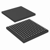
HSP50216KIZ Intersil, HSP50216KIZ Datasheet - Page 43

HSP50216KIZ
Manufacturer Part Number
HSP50216KIZ
Description
IC DOWNCONVERTER DGTL 4CH 196BGA
Manufacturer
Intersil
Datasheet
1.HSP50216KIZ.pdf
(58 pages)
Specifications of HSP50216KIZ
Function
Downconverter
Rf Type
W-CDMA
Package / Case
196-BGA
Lead Free Status / RoHS Status
Lead free / RoHS Compliant
P(31:0)
P(31:0)
P(15:0)
23:16
15:8
7:0
31
30
29
28
27
26
25
24
7
6
5
4
3
2
1
0
5
4
3
CH0 Ext AGC input enable. 0=CH0 loop filt, 1=external input.
CH1 Ext AGC input enable 0=CH1 loop filt, 1=external input.
CH2 Ext AGC input enable 0=CH2 loop filt, 1=external input.
CH3 Ext AGC input enable Set to 0.
CH0 enable serial output 1=FIR0 out enabled to serial outputs.
CH1 enable serial output 1=FIR1 out enabled to serial outputs.
CH2 enable serial output 1=FIR2 out enabled to serial outputs.
CH3 enable serial output 1=FIR3 out enabled to serial outputs.
When set, an interrupt will be generated on each data output of channel 0 to the output block. Typically, this bit will only be set for
one channel.
When set, the data input to the part will be disabled (the input enable will be zeroed and held at zero) on a μP reset (this is always
true for the reset pin, whether this bit is set or not, and additionally, the reset pin sets the input mode to gated). The input enable will
be released for the input sample that aligns with the SYNCI signal. This is a method for starting up the processing synchronous with
a particular data sample.
When this bit is set, the carrier center frequency will be updated from the holding register (IWA = *005h) to the active register on the
SYNCI signal. If the bit is set in register IWA = *004h to clear the phase accumulator feedback on loading, this function will
synchronize the phase of multiple channels. After initial synchronization, the bit in IWA = *004h can be cleared and updates will be
synchronous and phase continuous across channels.
When this bit is set, the FIR filter compute engine is reset on SYNCI. Resetting the FIR filter compute engine requires 32 clock (CLK)
cycles to initialize the read and write pointers.
When this bit is set, the AGC is reset on SYNCI.
This bit has the same function as bit 29, but for the timing (resampler) NCO. The bit to zero the phase accumulator feedback is in
register IWA = *00Ah.
When this bit is set, the CIC decimation counter is reset on SYNCI.
When this bit is set, the serial output block is reset on SYNCI. If bit 4 in location GWA F803h is set, the serial clock divider is also reset.
Same functions as 31:24 for channel 1.
Same functions as 31:24 for channel 2.
Same functions as 31:24 for channel 3.
When set to 1, this bit will keep the serial clock disabled after a hardware reset until receipt of the first SYNCI signal.
Enables resetting serial clock divider on SYNCI. When enabled, a SYNCI enabled for any of the four serial data outputs in the
Reset/Sync register (GWA = F802h, bits 24, 16, 8 or 0) will reset the serial clock divider.
SCLK polarity.
1
0
Clock low to high transition occurs at the center of the data bit.
Clock high to low transition at the center of the data bit.
TABLE 37. RESET/SYNC/INTERRUPT SOURCE SELECTION REGISTER (GWA = F802h)
TABLE 36. BUS ROUTING CONTROL REGISTER (GWA = F801h) (Continued)
43
TABLE 38. SERIAL CLOCK CONTROL REGISTER (GWA = F803h)
HSP50216
FUNCTION
FUNCTION
FUNCTION
August 17, 2007
FN4557.6


