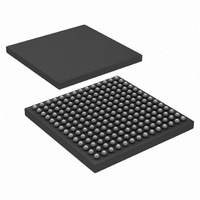
HSP50216KIZ Intersil, HSP50216KIZ Datasheet - Page 5

HSP50216KIZ
Manufacturer Part Number
HSP50216KIZ
Description
IC DOWNCONVERTER DGTL 4CH 196BGA
Manufacturer
Intersil
Datasheet
1.HSP50216KIZ.pdf
(58 pages)
Specifications of HSP50216KIZ
Function
Downconverter
Rf Type
W-CDMA
Package / Case
196-BGA
Lead Free Status / RoHS Status
Lead free / RoHS Compliant
Pin Descriptions
OUTPUTS
MICROPROCESSOR INTERFACE
μP MODE
ADD(2:0)
SYNCC
SYNCD
INTRPT
SYNCA
SYNCB
DSTRB
RD/WR
P(15:0)
NAME
SD1A
SD2A
SD1B
SD2B
SD1C
SD2C
SD1D
SD2D
SCLK
WR
RD
CE
or
or
TYPE
I/O
O
O
O
O
O
O
O
O
O
O
O
O
O
O
(Continued)
I
I
I
I
I
5
Serial Data Output 1A. A serial data stream output which can be programmed to consist of I1, Q1, I2, Q2,
magnitude, phase, frequency (dφ/dt), AGC gain, and/or zeros. In addition, data outputs from Channels 0,
1, 2 and 3 can be multiplexed into a common serial output data stream. Information can be sequenced in
a programmable order. See Serial Data Output Formatter Section.
Serial Data Output 2A. This output is provided as an auxiliary output for Serial Data Output 1A to route data
to a second destination or to output two words at a time for higher sample rates. SD2A has the same
programmability as SD1A except that floating point format is not available. See Serial Data Output
Formatter Section and Microprocessor Interface section.
Serial Data Output 1B. See description for SD1A.
Serial Data Output 2B. See description for SD2A.
Serial Data Output 1C. See description for SD1A.
Serial Data Output 2C. See description for SD2A.
Serial Data Output 1D. See description for SD1A.
Serial Data Output 2D. See description for SD2A.
Serial Output Clock. Can be programmed to be at 1, 1/2, 1/4, 1/8, or 1/16 times the clock frequency. The
polarity of SCLK is programmable.
Serial Data Output 1A sync signal. This signal is used to indicate the start of a data word and/or frame of
data. The polarity and position of SYNCA is programmable.
Serial Data Output 1B sync signal. This signal is used to indicate the start of a data word and/or frame of
data. The polarity and position of SYNCB is programmable.
Serial Data Output 1C sync signal. This signal is used to indicate the start of a data word and/or frame of
data. The polarity and position of SYNCC is programmable.
Serial Data Output 1D sync signal. This signal is used to indicate the start of a data word and/or frame of
data. The polarity and position of SYNCD is programmable.
Microprocessor Interface Data bus. See “Microprocessor Interface” on page 29. P15 is the MSB.
Microprocessor Interface Address bus. ADD2 is the MSB. See “Microprocessor Interface” on page 29.
Note: ADD2 is not used but designated for future expansion.
Microprocessor Interface Write or Data Strobe Signal. When the Microprocessor Interface Mode Control,
μP MODE, is a low data transfers (from either P(15:0) to the internal write holding register or from the
internal write holding register to the target register specified) occur on the low to high transition of WR when
CE is asserted (low). When the μP MODE control is high this input functions as a data read/write strobe.
In this mode with RD/WR low data transfers (from either P(15:0) to the internal write holding register or
from the internal write holding register to the target register specified) occur on the low to high transition of
Data Strobe. With RD/WR high the data from the address specified is placed on P(15:0) when Data Strobe
is low. See “Microprocessor Interface” on page 29.
Microprocessor Interface Read or Read/Write Signal. When the Microprocessor Interface Mode Control,
μP MODE, is a low the data from the address specified is placed on P(15:0) when RD is asserted (low)
and CE is asserted (low). When the μP MODE control is high this input functions as a Read/Write control
input. Data is read from P(15:0) when high or written to the appropriate register when low. See
“Microprocessor Interface” on page 29.
Microprocessor Interface Mode Control. This pin is used to select the Read/Write mode for the
Microprocessor Interface. Internally pulled down. See “Microprocessor Interface” on page 29.
Microprocessor Interface Chip Select. Active low. This pin has the same timing as the address pins.
Microprocessor Interrupt Signal. Asserted for a programmable number of clock cycles when new data is
available on the selected Channel.
HSP50216
DESCRIPTION
August 17, 2007
FN4557.6


