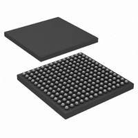
HSP50216KIZ Intersil, HSP50216KIZ Datasheet - Page 9

HSP50216KIZ
Manufacturer Part Number
HSP50216KIZ
Description
IC DOWNCONVERTER DGTL 4CH 196BGA
Manufacturer
Intersil
Datasheet
1.HSP50216KIZ.pdf
(58 pages)
Specifications of HSP50216KIZ
Function
Downconverter
Rf Type
W-CDMA
Package / Case
196-BGA
Lead Free Status / RoHS Status
Lead free / RoHS Compliant
NOTE:
Level Detector
An input level detector is provided to monitor the signal level
on any of the input busses. Which input bus, the input format,
and the level detection type are programmable (see
Microprocessor Interface section, Table 39, “INPUT LEVEL
DETECTOR SOURCE SELECT/FORMAT REGISTER (GWA
= F804h),” on page 44, Table 40, “INPUT LEVEL DETECTOR
CONFIGURATION REGISTER (GWA = F805h),” on page 45
and Table 41, “INPUT LEVEL DETECTOR START STROBE
REGISTER (GWA = F806h),” on page 45). This signal level
represents the wideband signal from the A/D and is useful for
controlling gain/attenuation blocks ahead of the converter.
The supported monitoring modes are: integrated magnitude
(like the HSP50214 without the threshold), leaky integration
(Y
(see GWA = F805h), and peak detection. The measurement
interval can be programmed from 2 to 65537 samples (or
continuous for the leaky integrator and peak detect cases).
The output is 32 bits and is read via the μP interface.
NCO/Mixer
After the input select/format section, the samples are
multiplied by quadrature sine wave samples from the carrier
NCO. The NCO has a 32-bit frequency control, providing
sub-hertz resolution at the maximum clock rate. The
quadrature sinusoids have exceptional purity. The purity of
the NCO should not be the determining factor for the
receiver dynamic range performance. The phase
quantization to the sine/cosine generator is 24 bits and the
amplitude quantization is 19 bits.
The carrier NCO center frequency is loaded via the μP bus.
The center frequency control is double buffered - the input is
loaded into a center frequency holding register via the μP
interface. The data is then transferred from the holding register
to the active register by a write to a address IWA *006h or by a
SYNCI signal, if loading via SYNCI is enabled. To synchronize
multiple channels, the carrier NCO phase accumulator
feedback can be zeroed on loading to restart all of the NCOs at
the same phase. A serial offset frequency input is also available
for each channel through the D(15:0) parallel data input bus (if
that bus is not needed for data input). This is legacy support for
HSP50210 type tracking signals. See IWA = *000 and *004 for
carrier offset frequency parameters.
5. Or 11, the exponent input saturates at 10.
00
01
10 (Note 5)
n
EXPONENT
= X
n
x A + Y
n-1
0
6
12
GAIN (dB)
x (1-A)) where A = 1, 2
14-BIT MODE: 14-BIT MANTISSA, 2-BIT EXPONENT, 12dB EXPONENT RANGE
9
X15
X15
X15
X15
X15
X14
-8
, 2
-12
X15
X14
X13
, or 2
X14
X13
X12
-16
HSP50216
PIN BIT WEIGHTING TO 16-BIT INPUT MAPPING
X13
X12
X11
X12
X10
X11
PN Value
After the mixers, a PN (pseudonoise) signal can be added to
the data. This feature is provided for test and to digitally reduce
the input sensitivity and adjust the receiver range (sensitivity).
The effect is the same as increasing the noise figure of the
receiver, reducing its sensitivity and overall dynamic range. For
testing, the PN generator provides a wideband signal which
may be used to verify the frequency response of a filter. The
one bit PN data is scaled by a 16-bit programmable scale
factor. The overall range for the PN is 0 to 1/4 full scale (see
IWA = *001h). A gain of 0 disables the PN input. The PN value
is formed as
where S is the PN generator output bit (treated as a sign bit)
and the 16 X’s refer to the PN Gain Register IWA = *001h.
The minimum, non-zero, PN value is 2
(-108dBFS) on each axis (-105dBFS total). For an input noise
level of -75dBFS, this allows the SNR to be decreased in
steps of 1/8dB or less. The I and Q PN codes are offset in time
to decorrelate them. The PN code is selected and enabled in
the test control register (F800h). The PN is added to the signal
after the mix with the three sign bits aligned with the most
significant three bits of the signal, so the maximum level is
-12dBFS and the minimum, non-zero level is -108dBFS. The
PN code can be 2
S S S
X10
X11
X9
2
X
-3
X10
X9
X8
2
X
-4 .
X X X X X X X X X X X X
15
X9
X8
X7
-1, 2
.
.
23
X8
X7
X6
.
-1 or 2
.
X7
X6
X5
.
15
.
-1 * 2
X6
X5
X4
.
-18
.
X5
X4
X3
23
of full scale
-1.
.
.
X4
X3
X2
.
August 17, 2007
2
X3
X2
0
-17
X
FN4557.6
2
X2
0
0
-18
X


