HSP50216KIZ Intersil, HSP50216KIZ Datasheet - Page 42
HSP50216KIZ
Manufacturer Part Number
HSP50216KIZ
Description
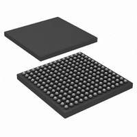
IC DOWNCONVERTER DGTL 4CH 196BGA
Manufacturer
Intersil
Datasheet
1.HSP50216KIZ.pdf
(58 pages)
Specifications of HSP50216KIZ
Function
Downconverter
Rf Type
W-CDMA
Package / Case
196-BGA
Lead Free Status / RoHS Status
Lead free / RoHS Compliant


NOTE: These Global Write Addresses control global functions on the HSP50216, so they are not repeated for each channel. The top five address
bits select this set of registers (F8XXh).
P(31:0)
P(31:0)
31:17
15:10
31:24
23:20
19:17
15:14
7:4
16
16
13
12
10
11
9
8
3
2
1
0
9
8
These bits can be routed to the output pins by setting bit 16 below. The bit to pin mapping is:
31 = Intrpt
28 = SYNCA
24 = SD1A
20 = SD2A
This is provided for testing board level interconnects. To control the SERCLK output, a divided down clock must be selected in the
serial clock control register (GWA = F803h).
This bit, when high, routes bits 31:17 to the output pins in place of the normal outputs. Bit 0 of this register must also be set to activate
this function.
Unused - set to zero.
Set-up time to CLOCK adjust. Adjusting the delay trades set up time for hold time. This bit is used to best center the delay without a
mask change.
Set-up time to WRITE adjust. Adjusting the delay trades set up time for hold time. This bit is used to best center the delay without a
mask change.
These bits, when set, route the MSB of the SIN output of the channel’s carrier NCO to the number 2 serial output pin in place of the
normal output.
Offset I PN by XORing bit 10 of the PN generator with the output PN.
Enable (2
sequence, a (2
the repeat period. Either or both generators can be disabled. The XORed output can further be XORed with a delayed version of the
(2
Enable (2
Test mode. When asserted, this bit puts the chip into internal (self) test mode.
Unused - set to zero.
Interrupt pulse width. The width of the interrupt pulse at the pin can be programmed to be from 1 to 15 clocks wide. Program with the
desired number of clocks. (NOTE: The pulse counter is only reset with the RESET pin. If a channel is reset by software or a SYNCI,
any interrupt pulse in process will finish).
DataRdy delay (CH1 only). Test. From 1-8.
CH1 or CH3 AGC to CH0 ext AGC. This bit selects whether the AGC loop filter output from CH1 or CH3 is routed to the external
AGC gain input of CH0. 0=CH3, 1=CH1.
CH3 ext source mux sel. These bits select whether the CH2 source mux, CIC2, or FIR2out is routed to the external input of FIR3.
0=CH2srcmux, 1=FIR2, 2=CIC2.
CH2 ext source mux sel. This bit selects whether the CH1 external source mux or FIR1out is routed to the external input of FIR2.
0=CH1srcmux, 1=FIR1out.
CH1 ext source mux sel. This bit selects whether the CIC0 output or FIR0out is routed to the external input of FIR1. 0=CIC0,
1=FIR0out.
CH0 backend input sel. 0=CIC0, 1=CIC1 (test).
CH1 backend input sel 0=CIC1, 1=CH1 ext src mux.
CH2 backend input sel 0=CIC2, 1=CH2 ext src mux.
CH3 backend input sel 0=CIC3, 1=CH3 ext source mux.
Tables of Global Write Address (GWA) Registers
23
- 1) sequence on the I channel to decorrelate it from the Q channel. Otherwise, the same sequence will be used on both I and Q.
23
15
- 1) PN generator. The PN signal that can be added to the mixer output of each channel is produced from a (2
- 1) PN generator.
15
30 = SYNCO
27 = SYNCB
23 = SD1B
19 = SD2B
7=CH0 6=CH1 5=CH2
- 1) sequence or both. Two separate generators are provided. The outputs of both are XORed together to extend
42
TABLE 36. BUS ROUTING CONTROL REGISTER (GWA = F801h)
TABLE 35. TEST CONTROL REGISTER (GWA = F800h)
29 = SERCLK (unless x1 CLK is selected)
26 = SYNCC
22 = SD1C
18 = SD2C
4=CH3.
HSP50216
25 = SYNCD
21 = SD1D
17 = SD2D
FUNCTION
FUNCTION
August 17, 2007
23
FN4557.6
- 1)
Related parts for HSP50216KIZ
Image
Part Number
Description
Manufacturer
Datasheet
Request
R

Part Number:
Description:
Intersil Corporation [CMOS Serial Controller Interface]
Manufacturer:
Intersil Corporation
Datasheet:
Part Number:
Description:
Manufacturer:
Intersil Corporation
Datasheet:
Part Number:
Description:
357-036-542-201 CARDEDGE 36POS DL .156 BLK LOPRO
Manufacturer:
Intersil Corporation
Datasheet:
Part Number:
Description:
1024-Word x 4-Bit LSI Static RAM
Manufacturer:
Intersil Corporation
Datasheet:
Part Number:
Description:
General Purpose NPN Transistor Arrays FN341.4
Manufacturer:
Intersil Corporation
Datasheet:
Part Number:
Description:
CMOS 16-Bit Microprocessor
Manufacturer:
Intersil Corporation
Datasheet:
Part Number:
Description:
Manufacturer:
Intersil Corporation
Datasheet:
Part Number:
Description:
Manufacturer:
Intersil Corporation
Datasheet:
Part Number:
Description:
Manufacturer:
Intersil Corporation
Datasheet:
Part Number:
Description:
Manufacturer:
Intersil Corporation
Datasheet:
Part Number:
Description:
CMOS 6-Bit Latch and Decoder Memory Interfaces
Manufacturer:
Intersil Corporation
Datasheet:
Part Number:
Description:
CA3046General Purpose NPN Transistor Arrays
Manufacturer:
Intersil Corporation
Datasheet:
Part Number:
Description:
Manufacturer:
Intersil Corporation
Datasheet:
Part Number:
Description:
TR909 DLC/FLC SLIC with Low Power Standby
Manufacturer:
Intersil Corporation
Datasheet:
Part Number:
Description:
Manufacturer:
Intersil Corporation
Datasheet: