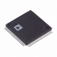
AD9857AST Analog Devices Inc, AD9857AST Datasheet - Page 24

AD9857AST
Manufacturer Part Number
AD9857AST
Description
IC QUADRATURE DGTL UPCONV 80LQFP
Manufacturer
Analog Devices Inc
Series
AD9857r
Datasheet
1.AD9857PCB.pdf
(40 pages)
Specifications of AD9857AST
Rohs Status
RoHS non-compliant
Function
Upconverter
Frequency
5MHz ~ 200MHz
Rf Type
HFC Cable Network
Package / Case
80-LQFP
Available stocks
Company
Part Number
Manufacturer
Quantity
Price
Company:
Part Number:
AD9857AST
Manufacturer:
AD
Quantity:
5 510
Company:
Part Number:
AD9857AST
Manufacturer:
SIEMENS
Quantity:
5 510
Company:
Part Number:
AD9857AST
Manufacturer:
ADI
Quantity:
255
Company:
Part Number:
AD9857ASTZ
Manufacturer:
AD
Quantity:
882
Part Number:
AD9857ASTZ
Manufacturer:
AD
Quantity:
20 000
AD9857
INPUT DATA PROGRAMMING
CONTROL INTERFACE—SERIAL I/O
The AD9857 serial port is a flexible, synchronous, serial
communications port allowing easy interface to many industry-
standard microcontrollers and microprocessors. The serial I/O
is compatible with most synchronous transfer formats,
including both the Motorola 6905/11 SPI and Intel 8051 SSR
protocols.
The interface allows read/write access to all registers that
configure the AD9857. Single or multiple byte transfers are
supported as well as MSB first or LSB first transfer formats. The
AD9857’s serial interface port can be configured as a single pin
I/O (SDIO) or two unidirectional pins for in/out (SDIO/SDO).
GENERAL OPERATION OF THE SERIAL INTERFACE
There are two phases to a communication cycle with the
AD9857. Phase 1 is the instruction cycle, which is the writing of
an instruction byte into the AD9857, coincident with the first
eight SCLK rising edges. The instruction byte provides the
AD9857 serial port controller with information regarding the
data transfer cycle, which is Phase 2 of the communication
cycle. The Phase 1 instruction byte defines whether the
upcoming data transfer is read or write, the number of bytes in
SCLK
SDIO
CS
SYMBOL
t
t
t
t
t
t
t
PRE
SCLK
DSU
SCLKPWH
SCLKPWL
DHLD
PRE
t
DSU
Figure 27. Timing Diagram for Data Write to AD9857
t
SCLKPWH
DEFINITION
CS SETUP TIME
PERIOD OF SERIAL DATA CLOCK
SERIAL DATA SETUP TIME
SERIAL DATA CLOCK PULSE WIDTH HIGH
SERIAL DATA CLOCK PULSE WIDTH LOW
SERIAL DATA HOLD TIME
1ST BIT
t
DHLD
t
SCLK
Rev. C | Page 24 of 40
t
SCLKPWL
the data transfer (1-4), and the starting register address for the
first byte of the data transfer.
The first eight SCLK rising edges of each communication cycle
are used to write the instruction byte into the AD9857. The
remaining SCLK edges are for Phase 2 of the communication
cycle. Phase 2 is the actual data transfer between the AD9857
and the system controller. Phase 2 of the communication cycle
is a transfer of 1, 2, 3, or 4 data bytes as determined by the
instruction byte. Typically, using one communication cycle in a
multibyte transfer is the preferred method. However, single-byte
communication cycles are useful to reduce CPU overhead when
register access requires one byte only. An example of this may
be to write the AD9857 SLEEP bit.
At the completion of any communication cycle, the AD9857
serial port controller expects the next eight rising SCLK edges
to be the instruction byte of the next communication cycle.
All data input to the AD9857 is registered on the rising edge of
SCLK. All data is driven out of the AD9857 on the falling edge
of SCLK.
Figure 27 and Figure 28 illustrate the data write and data read
operations on the AD9857 serial port. Figure 29 through
Figure 32 show the general operation of the AD9857 serial port.
2ND BIT
MIN
40ns
100ns
30ns
40ns
40ns
0ns


