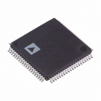
AD9857AST Analog Devices Inc, AD9857AST Datasheet - Page 33

AD9857AST
Manufacturer Part Number
AD9857AST
Description
IC QUADRATURE DGTL UPCONV 80LQFP
Manufacturer
Analog Devices Inc
Series
AD9857r
Datasheet
1.AD9857PCB.pdf
(40 pages)
Specifications of AD9857AST
Rohs Status
RoHS non-compliant
Function
Upconverter
Frequency
5MHz ~ 200MHz
Rf Type
HFC Cable Network
Package / Case
80-LQFP
Available stocks
Company
Part Number
Manufacturer
Quantity
Price
Company:
Part Number:
AD9857AST
Manufacturer:
AD
Quantity:
5 510
Company:
Part Number:
AD9857AST
Manufacturer:
SIEMENS
Quantity:
5 510
Company:
Part Number:
AD9857AST
Manufacturer:
ADI
Quantity:
255
Company:
Part Number:
AD9857ASTZ
Manufacturer:
AD
Quantity:
882
Part Number:
AD9857ASTZ
Manufacturer:
AD
Quantity:
20 000
If the user requires the PDCLK to continue running, the PLL
lock control bit (Control Register 00h<5>) can be set to a
Logic 1. When the PLL lock control bit is set, the PLL lock
indicator pin functionality remains the same, but the internal
operations noted in 1 through 5 above does not occur. The
default state of the PLL lock control bit is set, suppressing
internal monitoring of the PLL lock condition.
SINGLE OR DIFFERENTIAL CLOCK
In a noisy environment, a differential clock is usually considered
superior in performance over a single-ended clock in terms of
jitter performance, noise ingress, EMI, etc. However, sometimes
it is desirable (economy, layout, etc.) to use a single-ended clock.
The AD9857 allows the use of either a differential or single-
ended reference clock input signal. A logic high on the
DIFFCLKEN pin selects a differential clock input, whereas a
logic low on this pin selects a single-ended clock input. If a
differential clock is to be used, logic high is asserted on the
DIFFCLKEN pin. The reference clock signal is applied to the
REFCLK pin, and the inverted (complementary) reference clock
signal is applied to REFCLK . If a single-ended reference clock is
desired, logic low should be asserted on the DIFFCLKEN pin,
and the reference clock signal applied to REFCLK only.
REFCLK is ignored in single-ended mode, and can be left
floating or tied low.
CIC OVERFLOW PIN
Any condition that leads to an overflow of the CIC filters causes
signal activity on the CIC_OVRFL pin. The CIC_OVRFL pin
remains low (Logic 0) unless an overflow condition occurs.
When an overflow condition occurs, the CIC_OVRFL pin does
not remain high, but toggles in accordance with data going
through the CIC filter.
CLEARING THE CIC FILTER
The AD9857 CIC filter(s) can become corrupted if certain
illegal (nonvalid) operating conditions occur. If the CIC filter(s)
become corrupted, invalid results are apparent at the output and
the CIC_OVRFL output pin exhibits activity (toggling between
Logic 0 and Logic 1 in accordance with the data going through
the CIC filter). Examples of situations that may cause the CIC
filter to produce invalid results include:
1.
2.
3.
If the CIC filters become corrupted, the user can take advantage
of the CIC Clear bit (Control Register 00h<7>) to easily clear
the filter(s). By writing the CIC Clear bit to a Logic 1, the
AD9857 enters a routine that clears the entire data path,
including the CIC filter(s). The routine simply ignores the
Transmitting data when the PLL is not locked to the
reference frequency.
Operating the part above the maximum specified system
clock rate (200 MHz).
Changing the CIC filter interpolation rate during
transmission.
Rev. C| Page 33 of 40
D<13:0> pins and forces logical zeros on to the I and Q signal
processing paths while holding the CIC filter memory elements
reset. The routine is complete once all data path memory
elements are cleared. The CIC clear bit is also reset, so that the
user does not have to explicitly clear it.
NOTE: The time required to complete this routine is a function
of clock speed and the overall interpolation rate programmed
into the device. Higher interpolation rates create lower clock
frequencies at the filters preceding the CIC filter(s), causing the
routine time to increase.
In addition to the capability to detect and clear a corrupted CIC
filter condition, there are several conditions within the AD9857
that cause an automatic data path flush, which includes clearing
the CIC filter. The following conditions automatically clear the
signal processing chain of the AD9857:
1.
2.
3.
4.
DIGITAL POWER-DOWN
The AD9857 includes a digital power-down feature that can be
hardware- or software-controlled. Digital power-down allows
the users to save considerable operating power (60%–70%
reduction) when not transmitting and requires no startup time
before the next transmission can occur. The digital power-down
feature is ideal for burst mode applications where fast begin-to-
transmit time is required.
During digital power-down, the internal clock synchronization
is maintained and the PDCLK output continues to run.
Reduction in power is achieved by stopping many of the
internal clocks that drive the signal processing chain.
Invoking the digital power-down causes supply current
transients. Therefore, some users may not want to invoke the
DPD function to ease power supply regulation considerations.
Power-on reset—Proper initialization of the AD9857
requires the master reset pin to be active high for at least 5
REFCLK clock cycles. After master reset becomes inactive,
the AD9857 completes the data path clear routine as
described above.
PLL not locked to the reference clock—If the PLL lock
control bit is cleared and the AD9857 detects that the PLL
is not locked to the reference clock input, the AD9857
invokes and completes the data path clear routine after lock
has been detected. When the PLL lock control bit is set, the
data path clear routine is not invoked if the PLL is not
locked. The PLL lock control bit is set upon initialization,
disabling the clear routine functionality due to the PLL.
Digital power-down—When the DPD pin is driven high,
the AD9857 automatically invokes and completes the data
path clear routine before powering down the digital
section.
Full sleep mode—If the sleep mode control bit is set high,
the AD9857 automatically invokes and completes the data
path clear routine before powering down.
AD9857


