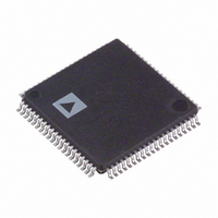
AD9857AST Analog Devices Inc, AD9857AST Datasheet - Page 34

AD9857AST
Manufacturer Part Number
AD9857AST
Description
IC QUADRATURE DGTL UPCONV 80LQFP
Manufacturer
Analog Devices Inc
Series
AD9857r
Datasheet
1.AD9857PCB.pdf
(40 pages)
Specifications of AD9857AST
Rohs Status
RoHS non-compliant
Function
Upconverter
Frequency
5MHz ~ 200MHz
Rf Type
HFC Cable Network
Package / Case
80-LQFP
Available stocks
Company
Part Number
Manufacturer
Quantity
Price
Company:
Part Number:
AD9857AST
Manufacturer:
AD
Quantity:
5 510
Company:
Part Number:
AD9857AST
Manufacturer:
SIEMENS
Quantity:
5 510
Company:
Part Number:
AD9857AST
Manufacturer:
ADI
Quantity:
255
Company:
Part Number:
AD9857ASTZ
Manufacturer:
AD
Quantity:
882
Part Number:
AD9857ASTZ
Manufacturer:
AD
Quantity:
20 000
AD9857
HARDWARE-CONTROLLED DIGITAL
POWER-DOWN
The hardware-controlled method for reducing power is to apply
a Logic 1 to the DPD pin. Restarting the part after a digital
power-down is accomplished by applying a Logic 0 to the DPD
pin. The DPD pin going to Logic 0 can occur simultaneously
with the activation of TxENABLE.
The user notices some time delay between invoking the digital
power-down function and the actual reduction in power. This is
due to an automatic routine that clears the signal processing
chain before stopping the clocks. Clearing the signal processing
chain before powering down ensures that the AD9857 is ready
to transmit when digital power-down mode is deactivated (see
the Clearing the CIC filter section for details).
SOFTWARE-CONTROLLED DIGITAL POWER-
DOWN
The software-controlled method for reducing digital power
between transmissions is simply an enable or disable of an
automatic power-down function. When enabled, digital power-
down between bursts occurs automatically after all data has
passed the AD9857 signal processing path.
When the AD9857 senses the TxENABLE input indicates the
end of a transmission, an on-chip timer is used to verify that the
data has completed transmission before stopping the internal
clocks that drive the signal processing chain memory elements.
As with the hardware activation method, clock synchronization
is maintained and the PDCLK output continues to run. An
active high signal on TxENABLE automatically restarts the
internal clocks, allowing the next burst transmission to start
immediately.
The automatic digital power-down between bursts is enabled by
writing the Control Register 01h<2> bit high. Writing the
Control Register 01h<2> bit low disables the function.
FULL SLEEP MODE
When coming out of full sleep mode, it is necessary to wait for
the PLL lock indicator to go high. Full Sleep mode functionality
is provided by programming one of the Control Registers
(01h<3>). When the Full-Sleep bit is set to a Logic 1, the device
shuts down both its digital and analog sections. During full
sleep mode, the contents of the registers of the AD9857 are
maintained. This mode yields the minimum possible device
power dissipation.
Rev. C | Page 34 of 40
POWER MANAGEMENT CONSIDERATIONS
The thermal impedance for the AD9857 80-lead LQFP package
is θ
using this value is calculated using ΔT = P × θ
The AD9857 power dissipation is at or below this value when
the SYSCLK frequency is at 200 MHz or lower with all optional
features enabled. The maximum power dissipation occurs while
operating the AD9857 as a quadrature modulator at the
maximum system clock frequency with TxENABLE in a logic
high state 100% of the time the device is powered. Under these
conditions, the device operates with all possible circuits enabled
at maximum speed.
Significant power saving may be seen by using a TxENABLE
signal that toggles low during times when the device does not
modulate.
The thermal impedance of the AD9857 package was measured
in a controlled temperature environment at temperatures
ranging from 28°C to 85°C with no air flow. The device under
test was soldered to an AD9857 evaluation board and operated
under conditions that generate maximum power dissipation.
The thermal resistance of a package can be thought of as a
thermal resistor that exists between the semiconductor surface
and the ambient air. The thermal impedance of a package is
determined by package material and its physical dimensions.
The dissipation of the heat from the package is directly
dependent upon the ambient air conditions and the physical
connection made between the IC package and the PCB.
Adequate dissipation of power from the AD9857 relies upon all
power and ground pins of the device being soldered directly to
copper planes on a PCB.
Many variables contribute to the operating junction
temperature within a device. They include:
1.
2.
3.
4.
5.
The power dissipation of the AD9857 in a given application is
determined by several operating conditions. Some of these
conditions, such as supply voltage and clock speed, have a direct
relationship with power dissipation. The most important factors
affecting power dissipation follow.
JA
Package style
Selection mode of operation
Internal system clock speed
Supply voltage
Ambient temperature
= 35°C/W. The maximum allowable power dissipation
P
P
P
=
=
=
. 1
Δ
150 −
θ
85
JA
T
35
W
85
JA
.


