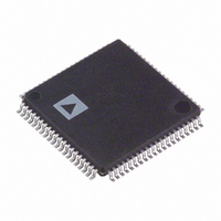
AD9857AST Analog Devices Inc, AD9857AST Datasheet - Page 30

AD9857AST
Manufacturer Part Number
AD9857AST
Description
IC QUADRATURE DGTL UPCONV 80LQFP
Manufacturer
Analog Devices Inc
Series
AD9857r
Datasheet
1.AD9857PCB.pdf
(40 pages)
Specifications of AD9857AST
Rohs Status
RoHS non-compliant
Function
Upconverter
Frequency
5MHz ~ 200MHz
Rf Type
HFC Cable Network
Package / Case
80-LQFP
Available stocks
Company
Part Number
Manufacturer
Quantity
Price
Company:
Part Number:
AD9857AST
Manufacturer:
AD
Quantity:
5 510
Company:
Part Number:
AD9857AST
Manufacturer:
SIEMENS
Quantity:
5 510
Company:
Part Number:
AD9857AST
Manufacturer:
ADI
Quantity:
255
Company:
Part Number:
AD9857ASTZ
Manufacturer:
AD
Quantity:
882
Part Number:
AD9857ASTZ
Manufacturer:
AD
Quantity:
20 000
AD9857
LATENCY
The latency through the AD9857 is easiest to describe in terms
of system clock (SYSCLK) cycles. Latency is a function of the
AD9857 configuration (that is, which mode and which optional
features are engaged). The latency is primarily affected by the
programmable interpolator’s rate.
The following values should be considered estimates because
observed latency may be data dependent. The latency was
calculated using the linear delay model for FIR filters.
Table 9.
Stage
Input Demux
Inverse CIC
Fixed Interpolator
Programmable
Interpolator
Quadrature Modulator
Inverse SINC
Output Scaler
Example
Interpolate mode
Clock multiplier = 4
Inverse CIC = On
Interpolate rate = 20
Inverse SINC = Off
Output scale = On
Latency for the Single-Tone Mode
In single-tone mode, frequency hopping is accomplished by
alternately selecting the two profile input pins. The time
required to switch from one frequency to another is less than 30
system clock cycles (SYSCLK) with the inverse SINC filter and
the output scaler engaged. With the inverse SINC filter
disengaged, the latency drops to less than 24 SYSCLK cycles.
Latency
System Clo
SYSCLK = REFCLK × Reference Clock Multiplier Factor
N = Programmable Interpolation Rate
=
cks/
+
(1 If Bypassed, 4–20)
(1 If Bypassed, 2–63)
(
8
9
×
4
20
+
=
488.75
)
6
+
=
(
12
1955
Reference
×
20
Modulator
Mode
4 × N
12 × N
(Optional)
72 × N
5 × N + 9
7
7 (Optional)
6 (Optional)
)
+
(
Clock Per
72
×
20
)
iods
+
Interpolator
Mode
8 × N
12 × N
(Optional)
72 × N
5 × N + 9
Not Used
7 (Optional)
6 (Optional)
(
5
×
20
)
Rev. C | Page 30 of 40
Other Factors Affecting Latency
Another factor affecting latency is the internal clock phase
relationship at the start of any burst transmission. For systems
that need to maintain exact SYSCLK cycle latency for all bursts,
the user must be aware of the possible difference in SYSCLK
cycle latency through the DEMUX, which precedes the signal
processing chain. The timing diagrams of Figure 33 and
Figure 34 describe how the latency differs depending upon the
phase relationship between the PDCLK and the clock that
samples data at the output of the data assembler logic (labeled
DEMUX on the block diagram).
Regarding Figure 33 and Figure 34, the SYSCLK/N trace
represents the clock frequency that is divided down from
SYSCLK by the CIC interpolation rate. That is, with SYSCLK
equal to 200 MHz and the CIC interpolation rate equal to
2 (N = 2), then SYSCLK/N equals 100 MHz. The SYSCLK/2N
and SYSCLK/4N signals are divided by 2 and 4 of SYSCLK/N,
respectively. For quadrature modulation mode, the PDCLK is
the SYSCLK/2N frequency and the clock that samples data into
the signal processing chain is the SYSCLK/4N frequency. Note
that SYSCLK/2N rising edges create the transition of the
SYSCLK/4N signal.
Figure 33 shows the timing for a burst transmission that starts
when the PDCLK (SYSCLK/2N) signal generates a rising edge
on the SYSCLK/4N clock. The latency from the D<13:0> pins to
the output of the data assembler logic is three PDCLK cycles.
The output is valid on the falling edge of SYSCLK/4N clock and
is sampled into the signal processing chain on the next rising
edge of the SYSCLK/4N clock (1/2 SYSCLK/4N clock cycle
latency).
Figure 34 shows the timing for a burst transmission that starts
when the PDCLK (SYSCLK/2N) signal generates a falling edge
on the SYSCLK/4N clock. The latency from the D<13:0> pins to
the output of the data assembler logic is three PDCLK cycles.
This is identical to Figure 33, but note that output is valid on the
rising edge of SYSCLK/4N clock and is sampled into the signal
processing chain on the next rising edge of the SYSCLK/4N
clock (1 full SYSCLK/4N clock cycle latency).
The difference in latency (as related to SYSCLK clock cycles) is
SYSCLK/2N, or one PDCLK cycle.


