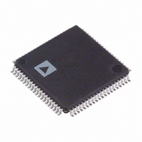
AD9857AST Analog Devices Inc, AD9857AST Datasheet - Page 32

AD9857AST
Manufacturer Part Number
AD9857AST
Description
IC QUADRATURE DGTL UPCONV 80LQFP
Manufacturer
Analog Devices Inc
Series
AD9857r
Datasheet
1.AD9857PCB.pdf
(40 pages)
Specifications of AD9857AST
Rohs Status
RoHS non-compliant
Function
Upconverter
Frequency
5MHz ~ 200MHz
Rf Type
HFC Cable Network
Package / Case
80-LQFP
Available stocks
Company
Part Number
Manufacturer
Quantity
Price
Company:
Part Number:
AD9857AST
Manufacturer:
AD
Quantity:
5 510
Company:
Part Number:
AD9857AST
Manufacturer:
SIEMENS
Quantity:
5 510
Company:
Part Number:
AD9857AST
Manufacturer:
ADI
Quantity:
255
Company:
Part Number:
AD9857ASTZ
Manufacturer:
AD
Quantity:
882
Part Number:
AD9857ASTZ
Manufacturer:
AD
Quantity:
20 000
AD9857
EASE OF USE FEATURES
PROFILE SELECT
The profile select pins, PS0 and PS1, activate one of four
internal profiles within the device. A profile is defined as a
group of control registers. The AD9857 contains four identical
register groupings associated with Profile 0, 1, 2, and 3. They are
available to the user to provide rapid changing of device
parameters via external hardware. Profiles are activated by
simply controlling the logic levels on device pins P0 and P1 as
defined in Table 10.
Table 10. Profile Select Matrix
PS1
0
0
1
1
Each profile offers the following functionality:
1.
2.
3.
4.
5.
The profile select pins are sampled synchronously with the
PDCLK signal for the quadrature modulation mode and the
interpolating DAC mode. For single-tone mode, they are
sampled synchronously with SYSCLK (internal only).
SETTING THE PHASE OF THE DDS
A feature unique to the AD9857 (versus previous ADI DDS
products) is the ability for the user to preset the DDS
accumulator to a value of 0. This sets the DDS outputs to
sin = 0 and cos = 1. To accomplish this, the user simply
programs a tuning word of 00000000h, which forces the DDS
core to a zero-phase condition.
REFERENCE CLOCK MULTIPLIER
For DDS applications, the carrier is typically limited to about
40% of SYSCLK. For a 65 MHz carrier, the system clock
required is above 160 MHz. To avoid the cost associated with
high frequency references, and the noise coupling issues
associated with operating a high frequency clock on a PC board,
the AD9857 provides an on-chip programmable clock
multiplier that multiplies the reference clock frequency supplied
to the part. The available clock multiplier range is from 4× to
Control of the DDS output frequency via the frequency
tuning word.
Control over the sum or difference of the quadrature
modulator components via the Spectral Invert bit (only
valid when the device is operating the quadrature
modulation mode).
Ability to bypass the inverse CIC filter.
Control of the CIC interpolation rate (1× to 63×), or
bypass CIC interpolator.
Control of the output scale factor (which offers a gain
range between 0 and 1.9921875.)
PS0
0
1
0
1
Profile
0
1
2
3
Rev. C | Page 32 of 40
20×, in integer steps. With the reference clock multiplier
enabled, the input reference clock required for the AD9857 can
be kept in the 10 MHz to 50 MHz range for 200 MHz system
operation, which results in cost and system implementation
savings. The reference clock multiplier function maintains clock
integrity as evidenced by the system phase noise characteristics
of the AD9857. External loop filter components consisting of a
series resistor (1.3 kΩ) and capacitor (0.01 µF) provide the
compensation zero for the REFCLK multiplier PLL loop. The
overall loop performance has been optimized for these
component values.
Control of the PLL is accomplished by programming the 5-bit
REFCLK multiplier portion of Control Register 00h.
The PLL may be bypassed by programming a value of 01h.
When bypassed, the PLL is shut down to conserve power.
When programmed for values ranging from 04h–14h (4–20
decimal), the PLL multiplies the REFCLK input frequency by
the corresponding decimal value. The maximum output
frequency of the PLL is restricted to 200 MHz. Whenever the
PLL value is changed, the user should be aware that time must
be allocated to allow the PLL to lock (approximately 1 ms).
Indication of the PLL’s lock status is provided externally via the
PLL lock indicator pin.
PLL LOCK
(See Reference Clock Multiplier section.)
The PLL lock indicator (PLL_LOCK) is an active high output
pin, serving as a flag to the user that the device has locked to the
REFCLK signal.
The status of the PLL lock indicator can be used to control
some housekeeping functions within the device if the user sets
the PLL lock control bit to 0 (Control Register 00h<5>).
Assuming that the PLL lock control bit is cleared (Logic 0), the
status of the PLL lock indicator pin has control over certain
internal device functions. Specifically, if the PLL lock indicator
is a Logic 0 (PLL not locked), then the following static
conditions apply:
1.
2.
3.
4.
5.
On the rising edge of the PLL Lock Indicator, the static
conditions mentioned above are removed and the device
assumes normal operation.
The accumulator in the DDS core is cleared.
The internal I and Q data paths are forced to a value of
ZERO.
The CIC filters are cleared.
The PDCLK is forced to a Logic 0.
Activity on the TxENABLE pin is ignored.


