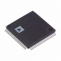
AD9857AST Analog Devices Inc, AD9857AST Datasheet - Page 27

AD9857AST
Manufacturer Part Number
AD9857AST
Description
IC QUADRATURE DGTL UPCONV 80LQFP
Manufacturer
Analog Devices Inc
Series
AD9857r
Datasheet
1.AD9857PCB.pdf
(40 pages)
Specifications of AD9857AST
Rohs Status
RoHS non-compliant
Function
Upconverter
Frequency
5MHz ~ 200MHz
Rf Type
HFC Cable Network
Package / Case
80-LQFP
Available stocks
Company
Part Number
Manufacturer
Quantity
Price
Company:
Part Number:
AD9857AST
Manufacturer:
AD
Quantity:
5 510
Company:
Part Number:
AD9857AST
Manufacturer:
SIEMENS
Quantity:
5 510
Company:
Part Number:
AD9857AST
Manufacturer:
ADI
Quantity:
255
Company:
Part Number:
AD9857ASTZ
Manufacturer:
AD
Quantity:
882
Part Number:
AD9857ASTZ
Manufacturer:
AD
Quantity:
20 000
When synchronization is lost between the system and the
AD9857, the SYNC I/O pin provides a means to re-establish
synchronization without reinitializing the entire chip. The
SYNC I/O pin enables the user to reset the AD9857 state
machine to accept the next eight SCLK rising edges to be
coincident with the instruction phase of a new communication
cycle. By applying and removing a “high” signal to the SYNC
I/O pin, the AD9857 is set to once again begin performing the
communication cycle in synchronization with the system. Any
information that had been written to the AD9857 registers
during a valid communication cycle prior to loss of
synchronization remains intact.
CONTROL REGISTER DESCRIPTIONS
Reference Clock (REFCLK) Multiplier—Register Address 00h,
Bits 0, 1, 2, 3, 4
A 5-bit number (M), the value of which determines the
multiplication factor for the internal PLL (Bit 4 is the MSB). The
system clock (SYSCLK) is M times the frequency of the
REFCLK input signal. If M = 01h, the PLL circuit is bypassed
and f
REFCLK frequency by M (4–20 decimal). Any other value of M
is considered an invalid entry.
PLL Lock Control—Register Address 00h, Bit 5
When set to a Logic 0, the device uses the status of the PLL lock
indicator pin to internally control the operation of the 14-bit
parallel data path. When set to a Logic 1, the internal control
logic ignores the status of the PLL lock indicator pin.
LSB First—Register Address 00h, Bit 6
When set to a Logic 1, the serial interface accepts serial data in
LSB first format. When set to a Logic 0, MSB first format is
assumed.
SDIO Input Only—Register Address 00h, Bit 7
When set to a Logic 1, the serial data I/O pin (SDIO) is
configured as an input only pin. When set to a Logic 0, the
SDIO pin has bidirectional operation.
Operating Mode—Register Address 01h, Bits 0, 1
00h: Selects the quadrature modulation mode of operation. 01h:
Selects the single-tone Mode of operation. 02h: Selects the
interpolating DAC mode of operation. 03h: Invalid entry.
Auto Power-Down—Register Address 01h, Bit 2
When set to a Logic 1, the device automatically switches into its
low power mode whenever TxENABLE is deasserted for a suf-
ficiently long period of time. When set to a Logic 0, the device
only powers down in response to the digital power-down pin.
SYSCLK
=f
REFCLK
. If 04h ≤ M ≤14h, the PLL multiplies the
Rev. C| Page 27 of 40
Full Sleep Mode—Register Address 01h, Bit 3
When set to a Logic 1, the device completely shuts down.
Reserved—Register Address 01h, Bit 4
Reserved—Register Address 01h, Bit 5
This bit must always be set to 0.
Inverse SINC Bypass—Register Address 01h, Bit 6
When set to a Logic 1, the inverse Sinc filter is BYPASSED.
When set to a Logic 0, the inverse Sinc filter is active.
CIC Clear—Register Address 01h, Bit 7
When set to a Logic 1, the CIC filters are cleared. When set to a
Logic 0, the CIC filters operate normally.
PROFILE #0
Tuning Word—Register Address 02h, Bits 0, 1, 2, 3, 4, 5, 6, 7
The lower byte of the 32-bit frequency tuning word, Bits 0–7.
Tuning Word—Register Address 03h, Bits 0, 1, 2, 3, 4, 5, 6, 7
The second byte of the 32-bit frequency tuning word, Bits 8–15.
Tuning Word—Register Address 04h, Bits 0,1, 2, 3, 4, 5, 6, 7
The third byte of the 32-bit frequency tuning word, Bits 16–23.
Tuning Word—Register Address 05h, Bits 0, 1, 2, 3, 4, 5, 6, 7
The fourth byte of the 32-bit frequency tuning word, Bits 24–31.
Inverse CIC Bypass—Register Address 06h, Bit 0
When set to a Logic 1, the inverse CIC filter is BYPASSED.
When set to a Logic 0, the inverse CIC filter is active.
Spectral Invert—Register Address 06h, Bit 1
The quadrature modulator takes the form:
I × cos(ω) + Q × sin(ω) when set to a Logic 1.
I × cos(ω) − Q × sin(ω) when set to a Logic 0.
CIC Interpolation Rate—Register Address 06h, Bits 2, 3, 4, 5,
6, 7
00h: Invalid entry.
01h: CIC filters BYPASSED.
02h–3Fh: CIC interpolation rate (2–63, decimal).
Output Scale Factor—Register Address 07h, Bits 0, 1, 2, 3, 4,
5, 6, 7
An 8-bit number that serves as a multiplier for the data pathway
before the data is delivered the DAC. It has an LSB weight of 2
(0.0078125). This yields a multiplier range of 0 to 1.9921875.
AD9857
–7


