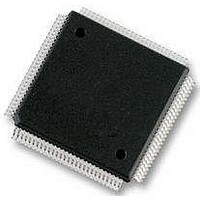
S9S12XS128J1MAL Freescale Semiconductor, S9S12XS128J1MAL Datasheet - Page 43

S9S12XS128J1MAL
Manufacturer Part Number
S9S12XS128J1MAL
Description
IC MCU 16BIT 128KB FLSH 112LQFP
Manufacturer
Freescale Semiconductor
Series
HCS12r
Datasheet
1.MC9S12XS64CAE.pdf
(738 pages)
Specifications of S9S12XS128J1MAL
Core Processor
HCS12X
Core Size
16-Bit
Speed
40MHz
Connectivity
CAN, SCI, SPI
Peripherals
LVD, POR, PWM, WDT
Number Of I /o
91
Program Memory Size
128KB (128K x 8)
Program Memory Type
FLASH
Eeprom Size
8K x 8
Ram Size
8K x 8
Voltage - Supply (vcc/vdd)
1.72 V ~ 5.5 V
Data Converters
A/D 16x12b
Oscillator Type
External
Operating Temperature
-40°C ~ 125°C
Package / Case
112-LQFP
Processor Series
S12XS
Core
HCS12
Data Bus Width
16 bit
Data Ram Size
8 KB
Interface Type
CAN, SCI, SPI
Maximum Clock Frequency
40 MHz
Number Of Programmable I/os
91
Number Of Timers
12
Maximum Operating Temperature
+ 125 C
Mounting Style
SMD/SMT
3rd Party Development Tools
EWHCS12
Development Tools By Supplier
DEMO9S12XSFAME, EVB9S12XEP100
Minimum Operating Temperature
- 40 C
On-chip Adc
12 bit, 16 Channel
Lead Free Status / RoHS Status
Lead free / RoHS Compliant
Available stocks
Company
Part Number
Manufacturer
Quantity
Price
Company:
Part Number:
S9S12XS128J1MAL
Manufacturer:
Freescale Semiconductor
Quantity:
10 000
- Current page: 43 of 738
- Download datasheet (4Mb)
1.2.3.18
PM[7:6] are a general-purpose input or output pins.
1.2.3.19
PM5 is a general-purpose input or output pin. It can be configured as the serial clock pin SCK of the serial
peripheral interface 0 (SPI0).
1.2.3.20
PM4 is a general-purpose input or output pin. It can be configured as the master output (during master
mode) or slave input pin (during slave mode) MOSI for the serial peripheral interface 0 (SPI0).
1.2.3.21
PM3 is a general-purpose input or output pin. It can be configured as the slave select pin SS of the serial
peripheral interface 0 (SPI0).
1.2.3.22
PM2 is a general-purpose input or output pin. It can be configured as the master input (during master
mode) or slave output pin (during slave mode) MISO for the serial peripheral interface 0 (SPI0).
1.2.3.23
PM1 is a general-purpose input or output pin. It can be configured as the transmit pin TXCAN of the
scalable controller area network controller 0 (CAN0). It can be configured as the transmit pin TXD of
serial communication interface 1 (SCI1).
1.2.3.24
PM0 is a general-purpose input or output pin. It can be configured as the receive pin RXCAN of the
scalable controller area network controller 0 (CAN0). It can be configured as the receive pin RXD of serial
communication interface 1 (SCI1).
1.2.3.25
PP7 is a general-purpose input or output pin. It can be configured as keypad wakeup input. It can be
configured as pulse width modulator (PWM) channel 7 output or emergency shutdown input.
1.2.3.26
PP[6:3] are a general-purpose input or output pins. They can be configured as keypad wakeup inputs. They
can be configured as pulse width modulator (PWM) channel 6-3 output.
Freescale Semiconductor
PM[7:6] — Port M I/O Pins 7-6
PM5 / SCK0 — Port M I/O Pin 5
PM4 / MOSI0 — Port M I/O Pin 4
PM3 / SS0 — Port M I/O Pin 3
PM2 / MISO0 — Port M I/O Pin 2
PM1 / TXCAN0 / TXD1 — Port M I/O Pin 1
PM0 / RXCAN0 / RXD1 — Port M I/O Pin 0
PP7 / KWP7 / PWM7 — Port P I/O Pin 7
PP[6:3] / KWP[6:3] / PWM[6:3] — Port P I/O Pins 6-3
S12XS Family Reference Manual, Rev. 1.11
Device Overview S12XS Family
43
Related parts for S9S12XS128J1MAL
Image
Part Number
Description
Manufacturer
Datasheet
Request
R
Part Number:
Description:
Manufacturer:
Freescale Semiconductor, Inc
Datasheet:
Part Number:
Description:
Manufacturer:
Freescale Semiconductor, Inc
Datasheet:
Part Number:
Description:
Manufacturer:
Freescale Semiconductor, Inc
Datasheet:
Part Number:
Description:
Manufacturer:
Freescale Semiconductor, Inc
Datasheet:
Part Number:
Description:
Manufacturer:
Freescale Semiconductor, Inc
Datasheet:
Part Number:
Description:
Manufacturer:
Freescale Semiconductor, Inc
Datasheet:
Part Number:
Description:
Manufacturer:
Freescale Semiconductor, Inc
Datasheet:
Part Number:
Description:
Manufacturer:
Freescale Semiconductor, Inc
Datasheet:
Part Number:
Description:
Manufacturer:
Freescale Semiconductor, Inc
Datasheet:
Part Number:
Description:
Manufacturer:
Freescale Semiconductor, Inc
Datasheet:
Part Number:
Description:
Manufacturer:
Freescale Semiconductor, Inc
Datasheet:
Part Number:
Description:
Manufacturer:
Freescale Semiconductor, Inc
Datasheet:
Part Number:
Description:
Manufacturer:
Freescale Semiconductor, Inc
Datasheet:
Part Number:
Description:
Manufacturer:
Freescale Semiconductor, Inc
Datasheet:
Part Number:
Description:
Manufacturer:
Freescale Semiconductor, Inc
Datasheet:


