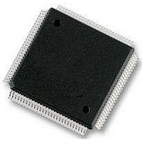
S9S12XS128J1MAL Freescale Semiconductor, S9S12XS128J1MAL Datasheet - Page 640

S9S12XS128J1MAL
Manufacturer Part Number
S9S12XS128J1MAL
Description
IC MCU 16BIT 128KB FLSH 112LQFP
Manufacturer
Freescale Semiconductor
Series
HCS12r
Datasheet
1.MC9S12XS64CAE.pdf
(738 pages)
Specifications of S9S12XS128J1MAL
Core Processor
HCS12X
Core Size
16-Bit
Speed
40MHz
Connectivity
CAN, SCI, SPI
Peripherals
LVD, POR, PWM, WDT
Number Of I /o
91
Program Memory Size
128KB (128K x 8)
Program Memory Type
FLASH
Eeprom Size
8K x 8
Ram Size
8K x 8
Voltage - Supply (vcc/vdd)
1.72 V ~ 5.5 V
Data Converters
A/D 16x12b
Oscillator Type
External
Operating Temperature
-40°C ~ 125°C
Package / Case
112-LQFP
Processor Series
S12XS
Core
HCS12
Data Bus Width
16 bit
Data Ram Size
8 KB
Interface Type
CAN, SCI, SPI
Maximum Clock Frequency
40 MHz
Number Of Programmable I/os
91
Number Of Timers
12
Maximum Operating Temperature
+ 125 C
Mounting Style
SMD/SMT
3rd Party Development Tools
EWHCS12
Development Tools By Supplier
DEMO9S12XSFAME, EVB9S12XEP100
Minimum Operating Temperature
- 40 C
On-chip Adc
12 bit, 16 Channel
Lead Free Status / RoHS Status
Lead free / RoHS Compliant
Available stocks
Company
Part Number
Manufacturer
Quantity
Price
Company:
Part Number:
S9S12XS128J1MAL
Manufacturer:
Freescale Semiconductor
Quantity:
10 000
- Current page: 640 of 738
- Download datasheet (4Mb)
64 KByte Flash Module (S12XFTMR64K1V1)
20.4.2
This section provides details of all available Flash commands launched by a command write sequence. The
ACCERR bit in the FSTAT register will be set during the command write sequence if any of the following
illegal steps are performed, causing the command not to be processed by the Memory Controller:
If a Flash block is read during execution of an algorithm (CCIF = 0) on that same block, the read operation
will return invalid data. If the SFDIF or DFDIF flags were not previously set when the invalid read
operation occurred, both the SFDIF and DFDIF flags will be set and the FECCR registers will be loaded
with the global address used in the invalid read operation with the data and parity fields set to all 0.
If the ACCERR or FPVIOL bits are set in the FSTAT register, the user must clear these bits before starting
any command write sequence (see
20.4.2.1
The Erase Verify All Blocks command will verify that all P-Flash and D-Flash blocks have been erased.
640
FCMD
0x0D
•
•
•
0x0B
0x0E
0x10
0x11
0x12
Starting any command write sequence that programs or erases Flash memory before initializing the
FCLKDIV register
Writing an invalid command as part of the command write sequence
For additional possible errors, refer to the error handling table provided for each command
Flash Command Description
Program D-Flash
Set User Margin
Set Field Margin
D-Flash Section
Unsecure Flash
Erase Verify All Blocks Command
Erase D-Flash
Erase Verify
A Flash word or phrase must be in the erased state before being
programmed. Cumulative programming of bits within a Flash word or
phrase is not allowed.
Command
Sector
Level
Level
Table 20-31. Erase Verify All Blocks Command FCCOB Requirements
CCOBIX[2:0]
000
Supports a method of releasing MCU security by erasing all D-Flash (and P-Flash) blocks
and verifying that all D-Flash (and P-Flash) blocks are erased.
Specifies a user margin read level for the D-Flash block.
Specifies a field margin read level for the D-Flash block (special modes only).
Verify that a given number of words starting at the address provided are erased.
Program up to four words in the D-Flash block.
Erase all bytes in a sector of the D-Flash block.
S12XS Family Reference Manual, Rev. 1.11
Section
Table 20-30. D-Flash Commands
20.3.2.7).
0x01
CAUTION
FCCOB Parameters
Function on D-Flash Memory
Not required
Freescale Semiconductor
Related parts for S9S12XS128J1MAL
Image
Part Number
Description
Manufacturer
Datasheet
Request
R
Part Number:
Description:
Manufacturer:
Freescale Semiconductor, Inc
Datasheet:
Part Number:
Description:
Manufacturer:
Freescale Semiconductor, Inc
Datasheet:
Part Number:
Description:
Manufacturer:
Freescale Semiconductor, Inc
Datasheet:
Part Number:
Description:
Manufacturer:
Freescale Semiconductor, Inc
Datasheet:
Part Number:
Description:
Manufacturer:
Freescale Semiconductor, Inc
Datasheet:
Part Number:
Description:
Manufacturer:
Freescale Semiconductor, Inc
Datasheet:
Part Number:
Description:
Manufacturer:
Freescale Semiconductor, Inc
Datasheet:
Part Number:
Description:
Manufacturer:
Freescale Semiconductor, Inc
Datasheet:
Part Number:
Description:
Manufacturer:
Freescale Semiconductor, Inc
Datasheet:
Part Number:
Description:
Manufacturer:
Freescale Semiconductor, Inc
Datasheet:
Part Number:
Description:
Manufacturer:
Freescale Semiconductor, Inc
Datasheet:
Part Number:
Description:
Manufacturer:
Freescale Semiconductor, Inc
Datasheet:
Part Number:
Description:
Manufacturer:
Freescale Semiconductor, Inc
Datasheet:
Part Number:
Description:
Manufacturer:
Freescale Semiconductor, Inc
Datasheet:
Part Number:
Description:
Manufacturer:
Freescale Semiconductor, Inc
Datasheet:


