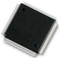
S9S12XS128J1MAL Freescale Semiconductor, S9S12XS128J1MAL Datasheet - Page 455

S9S12XS128J1MAL
Manufacturer Part Number
S9S12XS128J1MAL
Description
IC MCU 16BIT 128KB FLSH 112LQFP
Manufacturer
Freescale Semiconductor
Series
HCS12r
Datasheet
1.MC9S12XS64CAE.pdf
(738 pages)
Specifications of S9S12XS128J1MAL
Core Processor
HCS12X
Core Size
16-Bit
Speed
40MHz
Connectivity
CAN, SCI, SPI
Peripherals
LVD, POR, PWM, WDT
Number Of I /o
91
Program Memory Size
128KB (128K x 8)
Program Memory Type
FLASH
Eeprom Size
8K x 8
Ram Size
8K x 8
Voltage - Supply (vcc/vdd)
1.72 V ~ 5.5 V
Data Converters
A/D 16x12b
Oscillator Type
External
Operating Temperature
-40°C ~ 125°C
Package / Case
112-LQFP
Processor Series
S12XS
Core
HCS12
Data Bus Width
16 bit
Data Ram Size
8 KB
Interface Type
CAN, SCI, SPI
Maximum Clock Frequency
40 MHz
Number Of Programmable I/os
91
Number Of Timers
12
Maximum Operating Temperature
+ 125 C
Mounting Style
SMD/SMT
3rd Party Development Tools
EWHCS12
Development Tools By Supplier
DEMO9S12XSFAME, EVB9S12XEP100
Minimum Operating Temperature
- 40 C
On-chip Adc
12 bit, 16 Channel
Lead Free Status / RoHS Status
Lead free / RoHS Compliant
Available stocks
Company
Part Number
Manufacturer
Quantity
Price
Company:
Part Number:
S9S12XS128J1MAL
Manufacturer:
Freescale Semiconductor
Quantity:
10 000
- Current page: 455 of 738
- Download datasheet (4Mb)
The SS line can remain active low between successive transfers (can be tied low at all times). This format
is sometimes preferred in systems having a single fixed master and a single slave that drive the MISO data
line.
The SPI interrupt request flag (SPIF) is common to both the master and slave modes. SPIF gets set one
half SCK cycle after the last SCK edge.
15.4.4
Baud rate generation consists of a series of divider stages. Six bits in the SPI baud rate register (SPPR2,
SPPR1, SPPR0, SPR2, SPR1, and SPR0) determine the divisor to the SPI module clock which results in
the SPI baud rate.
The SPI clock rate is determined by the product of the value in the baud rate preselection bits
(SPPR2–SPPR0) and the value in the baud rate selection bits (SPR2–SPR0). The module clock divisor
equation is shown in
Freescale Semiconductor
•
End of Idle State
SCK Edge Number
SCK (CPOL = 0)
SCK (CPOL = 1)
SAMPLE I
MOSI/MISO
CHANGE O
CHANGE O
SEL SS (O)
Master only
SEL SS (I)
t
t
t
Figure 15-15. SPI Clock Format 1 (CPHA = 1), with 16-Bit Transfer Width selected (XFRW = 1)
MOSI pin
MISO pin
L
T
I
Back-to-back transfers in master mode
In master mode, if a transmission has completed and new data is available in the SPI data register,
this data is sent out immediately without a trailing and minimum idle time.
MSB first (LSBFE = 0)
LSB first (LSBFE = 1)
= Minimum idling time between transfers (minimum SS high time), not required for back-to-back transfers
= Minimum leading time before the first SCK edge, not required for back-to-back transfers
= Minimum trailing time after the last SCK edge
SPI Baud Rate Generation
Equation
t
L
1
MSB
LSB
2
BaudRateDivisor = (SPPR + 1) • 2
3
Bit 14
Bit 1
4
15-3.
5
Bit 13
Begin
Bit 2
S12XS Family Reference Manual, Rev. 1.11
6
7
Bit 12
Bit 3
8
9
Bit 11
Bit 4
10
11
Bit 10 Bit 9 Bit 8 Bit 7 Bit 6
Bit 5
12
13
Bit 6
14
Transfer
15
Bit 7 Bit 8 Bit 9 Bit 10Bit 11Bit 12Bit 13Bit 14
16
17
18
19
20
(SPR + 1)
21
Bit 5
22
23
Bit 4 Bit 3 Bit 2 Bit 1
24
25
End
26
27
Serial Peripheral Interface (S12SPIV5)
28
29
30
31
MSB
LSB
32
t
T
Begin of Idle State
t
I
Minimum 1/2 SCK
for t
t
L
T
, t
l
, t
L
Eqn. 15-3
455
Related parts for S9S12XS128J1MAL
Image
Part Number
Description
Manufacturer
Datasheet
Request
R
Part Number:
Description:
Manufacturer:
Freescale Semiconductor, Inc
Datasheet:
Part Number:
Description:
Manufacturer:
Freescale Semiconductor, Inc
Datasheet:
Part Number:
Description:
Manufacturer:
Freescale Semiconductor, Inc
Datasheet:
Part Number:
Description:
Manufacturer:
Freescale Semiconductor, Inc
Datasheet:
Part Number:
Description:
Manufacturer:
Freescale Semiconductor, Inc
Datasheet:
Part Number:
Description:
Manufacturer:
Freescale Semiconductor, Inc
Datasheet:
Part Number:
Description:
Manufacturer:
Freescale Semiconductor, Inc
Datasheet:
Part Number:
Description:
Manufacturer:
Freescale Semiconductor, Inc
Datasheet:
Part Number:
Description:
Manufacturer:
Freescale Semiconductor, Inc
Datasheet:
Part Number:
Description:
Manufacturer:
Freescale Semiconductor, Inc
Datasheet:
Part Number:
Description:
Manufacturer:
Freescale Semiconductor, Inc
Datasheet:
Part Number:
Description:
Manufacturer:
Freescale Semiconductor, Inc
Datasheet:
Part Number:
Description:
Manufacturer:
Freescale Semiconductor, Inc
Datasheet:
Part Number:
Description:
Manufacturer:
Freescale Semiconductor, Inc
Datasheet:
Part Number:
Description:
Manufacturer:
Freescale Semiconductor, Inc
Datasheet:


