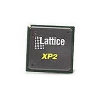
LFXP2-8E-5FTN256C Lattice, LFXP2-8E-5FTN256C Datasheet - Page 109

LFXP2-8E-5FTN256C
Manufacturer Part Number
LFXP2-8E-5FTN256C
Description
FPGA - Field Programmable Gate Array 8K LUTs 201I/O Inst- on DSP 1.2V -5 Spd
Manufacturer
Lattice
Datasheet
1.LFXP2-8E-5FTN256I.pdf
(341 pages)
Specifications of LFXP2-8E-5FTN256C
Number Of Macrocells
8000
Number Of Programmable I/os
201
Data Ram Size
226304
Supply Voltage (max)
1.26 V
Maximum Operating Temperature
+ 85 C
Minimum Operating Temperature
0 C
Mounting Style
SMD/SMT
Supply Voltage (min)
1.14 V
Package / Case
FTBGA-256
Lead Free Status / RoHS Status
Lead free / RoHS Compliant
Available stocks
Company
Part Number
Manufacturer
Quantity
Price
Company:
Part Number:
LFXP2-8E-5FTN256C
Manufacturer:
Lattice
Quantity:
63
Company:
Part Number:
LFXP2-8E-5FTN256C
Manufacturer:
Lattice Semiconductor Corporation
Quantity:
10 000
- Current page: 109 of 341
- Download datasheet (10Mb)
Lattice Semiconductor
Prior to device configuration, the ratioed input thresholds always tracks the bank V
effect after configuration. Output standards within a bank are always set by V
dards that can be mixed in the same bank.
Table 8-4. Mixed Voltage Support
sysIO Standards Supported by Bank
Table 8-5. I/O Standards Supported by Bank
I/O Buffers
Output Standards
Supported
Inputs
Clock Inputs
PCI Support
LVDS Output Buffers
1. These differential standards are implemented by using a complementary LVCMOS driver with external resistor pack.
2. Available only on 50% of the I/Os in the bank.
V
1.2V
1.5V
1.8V
2.5V
3.3V
CCIO
Description
1.2V
Yes
Yes
Yes
Yes
Yes
Single-ended
LVTTL
LVCMOS33
LVCMOS25
LVCMOS18
LVCMOS15
LVCMOS12
SSTL18 Class I, II
SSTL25 Class I, II
SSTL33 Class I, II
HSTL15 Class I
HSTL18_I, II
SSTL18D Class I, II
SSTL25D Class I, II
SSTL33D Class I, II
HSTL15D Class I
HSTL18D Class I, II
MLVDS
LVDS25E
LVPECL
BLVDS
RSDS
All Single-ended,
Differential
All Single-ended,
Differential
PCI33 with clamp
1.5V
Yes
Input sysIO Standards
Banks 0-1
1
1
Top Side
1
1
1.8V
Yes
Single-ended and
Differential
LVTTL
LVCMOS33
LVCMOS25
LVCMOS18
LVCMOS15
LVCMOS12
SSTL18 Class I, II
SSTL25 Class I, II
SSTL33 Class I, II
HSTL15 Class I
HSTL18 Class I, II
SSTL18D Class I, II
SSTL25D Class I, II
SSTL33D Class I, II
HSTL15D Class I
HSTL18D Class I, II
MLVDS
LVDS
LVDS25E
LVPECL
BLVDS
RSDS
All Single-ended,
Differential
All Single-ended,
Differential
PCI33 without clamp
LVDS (3.5mA) Buffers
2.5V
Yes
Yes
Yes
Yes
Yes
Right Side
1
Banks 2-3
1
1
1
3.3V
Yes
Yes
Yes
Yes
Yes
8-5
2
1.2V
Single-ended
LVTTL
LVCMOS33
LVCMOS25
LVCMOS18
LVCMOS15
LVCMOS12
SSTL18 Class I, II
SSTL2 Class I, II
SSTL3 Class I, II
HSTL15 Class I
HSTL18 Class I, II
SSTL18D Class I, II
SSTL25D Class I, II,
SSTL33D Class I, II
HSTL15D Class I
HSTL18D Class I, II
MLVDS
LVDS25E
LVPECL
BLVDS
RSDS
All Single-ended,
Differential
All Single-ended,
Differential
PCI33 with clamp
Yes
Bottom Side
1
Banks 4-5
1
1
1
LatticeXP2 sysIO Usage Guide
1.5V
Yes
CCIO
Output sysIO Standards
. Table 8-4 shows the sysIO stan-
CCIO
1.8V
Yes
Single-ended and
Differential
LVTTL
LVCMOS33
LVCMOS25
LVCMOS18
LVCMOS15
LVCMOS12
SSTL18 Class I
SSTL2 Class I, II
SSTL3 Class I, II
HSTL15 Class I, III
HSTL18 Class I, II, III
SSTL18D Class I,
SSTL25D Class I, II,
SSTL33D_I, II
HSTL15D Class I
HSTL18D Class I, II
MLVDS
LVDS
LVDS25E
LVPECL
BLVDS
RSDS
All Single-ended,
Differential
All Single-ended,
Differential
PCI33 without clamp
LVDS (3.5mA) Buffers
. This option only takes
1
1
1
Banks 6-7
1
Left Side
2.5V
Yes
3.3V
2
Yes
Related parts for LFXP2-8E-5FTN256C
Image
Part Number
Description
Manufacturer
Datasheet
Request
R

Part Number:
Description:
FPGA - Field Programmable Gate Array 8K LUTs 100I/O Inst- on DSP 1.2V -5 Spd
Manufacturer:
Lattice
Datasheet:

Part Number:
Description:
FPGA - Field Programmable Gate Array 8K LUTs 201 I/O Inst on DSP 1.2V -5 Spd
Manufacturer:
Lattice
Datasheet:

Part Number:
Description:
FPGA - Field Programmable Gate Array 8K LUTs 100 I/O Inst on DSP 1.2V -5 Spd
Manufacturer:
Lattice
Datasheet:

Part Number:
Description:
IC, LATTICEXP2 FPGA, 435MHZ, QFP-208
Manufacturer:
LATTICE SEMICONDUCTOR
Datasheet:

Part Number:
Description:
FPGA - Field Programmable Gate Array 8K LUTs 86I/O Inst- on DSP 1.2V -5 Spd
Manufacturer:
Lattice

Part Number:
Description:
FPGA - Field Programmable Gate Array 8K LUTs 201I/O Inst- on DSP 1.2V -7 Spd
Manufacturer:
Lattice
Datasheet:
Part Number:
Description:
FPGA LatticeXP2 Family 8000 Cells Flash Technology 1.2V 144-Pin TQFP
Manufacturer:
LATTICE SEMICONDUCTOR
Datasheet:

Part Number:
Description:
IC DSP 8KLUTS 146I/O 208PQFP
Manufacturer:
Lattice
Datasheet:

Part Number:
Description:
IC DSP 8KLUTS 100I/O 144TQFP
Manufacturer:
Lattice
Datasheet:

Part Number:
Description:
IC DSP 8KLUTS 86I/O 132CSBGA
Manufacturer:
Lattice
Datasheet:

Part Number:
Description:
IC DSP 8KLUTS 86I/O 132CSBGA
Manufacturer:
Lattice
Datasheet:

Part Number:
Description:
IC DSP 8KLUTS 146I/O 208PQFP
Manufacturer:
Lattice
Datasheet:

Part Number:
Description:
IC DSP 8KLUTS 201I/O 256FTBGA
Manufacturer:
Lattice
Datasheet:

Part Number:
Description:
IC FPGA 8KLUTS 86I/O 132-BGA
Manufacturer:
Lattice
Datasheet:

Part Number:
Description:
IC FPGA 8KLUTS 86I/O 132-BGA
Manufacturer:
Lattice
Datasheet:


