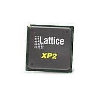
LFXP2-8E-5FTN256C Lattice, LFXP2-8E-5FTN256C Datasheet - Page 338

LFXP2-8E-5FTN256C
Manufacturer Part Number
LFXP2-8E-5FTN256C
Description
FPGA - Field Programmable Gate Array 8K LUTs 201I/O Inst- on DSP 1.2V -5 Spd
Manufacturer
Lattice
Datasheet
1.LFXP2-8E-5FTN256I.pdf
(341 pages)
Specifications of LFXP2-8E-5FTN256C
Number Of Macrocells
8000
Number Of Programmable I/os
201
Data Ram Size
226304
Supply Voltage (max)
1.26 V
Maximum Operating Temperature
+ 85 C
Minimum Operating Temperature
0 C
Mounting Style
SMD/SMT
Supply Voltage (min)
1.14 V
Package / Case
FTBGA-256
Lead Free Status / RoHS Status
Lead free / RoHS Compliant
Available stocks
Company
Part Number
Manufacturer
Quantity
Price
Company:
Part Number:
LFXP2-8E-5FTN256C
Manufacturer:
Lattice
Quantity:
63
Company:
Part Number:
LFXP2-8E-5FTN256C
Manufacturer:
Lattice Semiconductor Corporation
Quantity:
10 000
- Current page: 338 of 341
- Download datasheet (10Mb)
Lattice Semiconductor
LatticeXP2 Hardware Checklist
DDR/DDR2 Memory Interface Pin Assignments
The DDR Memory interface on the LatticeXP2 device family is provided with a pre-engineered I/O register along
with the precision I/O DLL timing control. There are two I/O DLL specifically assigned to the two halves of the
device. One I/O DLL supports I/O banks 1, 2, 3 and 4; another I/O DLL supports I/O banks 0, 5, 6 and 7.
In addition to the I/O DLL assignments, there are pre-defined data strobes (DQS) signals that can support a span
of I/O pins as part of the memory data lanes. When assigning DDR memory interface I/O pins, the FPGA designer
must insure that there is enough I/O pins to assign DDR memory data pins for each of the assigned DQS signals.
True-LVDS Output Pin Assignments
True-LVDS outputs are available on 50% of the I/O pins on the left and right sides of the device. The left and right
side I/O banks are banks 2, 3, 6 and 7. When using the LVDS outputs, a 2.5V supply needs to be connected to
these VCCIO supply rails.
HSTL and SSTL Pin Assignments
These externally referenced I/O standards require an external reference voltage. Each of the LatticeXP2 device
family I/O banks allows up to two pre-defined V
pins. The V
pin(s) should get the highest priority for pin
REF
REF
assignment.
PCI Clamp Pin Assignment
PCI clamps are available on the top and bottom sides of the device. When the system design calls for PCI clamp,
those pins should be assigned to I/O banks 0, 1, 4 and 5. For the clamp characteristic, refer to the IBIS buffer mod-
els either on the Lattice website at
www.latticesemi.com
or in the ispLEVER design tool.
Test Output Enable (TOE)
TOE signal is used to tri-state all I/O pins and override the functional outputs for board level test. It is recommended
to have a pull-up resistor to make sure that when not in use, the TOE will not interfere with the normal functionality
of the I/O pins.
18-4
Related parts for LFXP2-8E-5FTN256C
Image
Part Number
Description
Manufacturer
Datasheet
Request
R

Part Number:
Description:
FPGA - Field Programmable Gate Array 8K LUTs 100I/O Inst- on DSP 1.2V -5 Spd
Manufacturer:
Lattice
Datasheet:

Part Number:
Description:
FPGA - Field Programmable Gate Array 8K LUTs 201 I/O Inst on DSP 1.2V -5 Spd
Manufacturer:
Lattice
Datasheet:

Part Number:
Description:
FPGA - Field Programmable Gate Array 8K LUTs 100 I/O Inst on DSP 1.2V -5 Spd
Manufacturer:
Lattice
Datasheet:

Part Number:
Description:
IC, LATTICEXP2 FPGA, 435MHZ, QFP-208
Manufacturer:
LATTICE SEMICONDUCTOR
Datasheet:

Part Number:
Description:
FPGA - Field Programmable Gate Array 8K LUTs 86I/O Inst- on DSP 1.2V -5 Spd
Manufacturer:
Lattice

Part Number:
Description:
FPGA - Field Programmable Gate Array 8K LUTs 201I/O Inst- on DSP 1.2V -7 Spd
Manufacturer:
Lattice
Datasheet:
Part Number:
Description:
FPGA LatticeXP2 Family 8000 Cells Flash Technology 1.2V 144-Pin TQFP
Manufacturer:
LATTICE SEMICONDUCTOR
Datasheet:

Part Number:
Description:
IC DSP 8KLUTS 146I/O 208PQFP
Manufacturer:
Lattice
Datasheet:

Part Number:
Description:
IC DSP 8KLUTS 100I/O 144TQFP
Manufacturer:
Lattice
Datasheet:

Part Number:
Description:
IC DSP 8KLUTS 86I/O 132CSBGA
Manufacturer:
Lattice
Datasheet:

Part Number:
Description:
IC DSP 8KLUTS 86I/O 132CSBGA
Manufacturer:
Lattice
Datasheet:

Part Number:
Description:
IC DSP 8KLUTS 146I/O 208PQFP
Manufacturer:
Lattice
Datasheet:

Part Number:
Description:
IC DSP 8KLUTS 201I/O 256FTBGA
Manufacturer:
Lattice
Datasheet:

Part Number:
Description:
IC FPGA 8KLUTS 86I/O 132-BGA
Manufacturer:
Lattice
Datasheet:

Part Number:
Description:
IC FPGA 8KLUTS 86I/O 132-BGA
Manufacturer:
Lattice
Datasheet:


