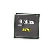
LFXP2-8E-5FTN256C Lattice, LFXP2-8E-5FTN256C Datasheet - Page 136

LFXP2-8E-5FTN256C
Manufacturer Part Number
LFXP2-8E-5FTN256C
Description
FPGA - Field Programmable Gate Array 8K LUTs 201I/O Inst- on DSP 1.2V -5 Spd
Manufacturer
Lattice
Datasheet
1.LFXP2-8E-5FTN256I.pdf
(341 pages)
Specifications of LFXP2-8E-5FTN256C
Number Of Macrocells
8000
Number Of Programmable I/os
201
Data Ram Size
226304
Supply Voltage (max)
1.26 V
Maximum Operating Temperature
+ 85 C
Minimum Operating Temperature
0 C
Mounting Style
SMD/SMT
Supply Voltage (min)
1.14 V
Package / Case
FTBGA-256
Lead Free Status / RoHS Status
Lead free / RoHS Compliant
Available stocks
Company
Part Number
Manufacturer
Quantity
Price
Company:
Part Number:
LFXP2-8E-5FTN256C
Manufacturer:
Lattice
Quantity:
63
Company:
Part Number:
LFXP2-8E-5FTN256C
Manufacturer:
Lattice Semiconductor Corporation
Quantity:
10 000
- Current page: 136 of 341
- Download datasheet (10Mb)
Lattice Semiconductor
Figure 9-10. Clock Injection Delay Removal Application
PLL Clock Phase Adjustment
In this mode the PLL is used to create fixed phase relationships in 22.5° increments. Creating fixed phase relation-
ships is useful for forward clock interfaces where a specific relationship between clock and data is required.
The fixed phase relationship can be used between CLKI and CLKOS or between CLKOP and CLKOS.
Figure 9-11. CLKOS Phase Adjustment from CLKOP
IPexpress Output
There are two IPexpress outputs that are important for use in the design. The first is the <module_name>.[v|vhd]
file. This is the user-named module that was generated by the tool to be used in both synthesis and simulation
flows. The second is a template file, <module_name>_tmpl.[v|vhd]. This file contains a sample instantiation of the
module. This file is provided for the user to copy/paste the instance and is not intended to be used in the synthesis
or simulation flows directly.
For the PLL, IPexpress sets attributes in the HDL module that are specific to the data rate selected. Although these
attributes can be easily changed, they should only be modified by re-running the GUI so that the performance of
the PLL is maintained. After the map stage in the design flow, FREQUENCY preferences will be included in the
preference file to automatically constrain the clocks produced from the PLL.
CLKI
CLKFB
CLKI
CLKOP
CLKOS with 90°
Phase Shift
CLKI
CLKFB
CLKI
Clock at
Clock Tree
without PLL
CLKOP/CLKOS
at Clock Tree
with PLL
PLL
PLL
Clock Injection Delay
9-14
CLKOP
CLKOP
CLKOS
Clock Tree
LatticeXP2 sysCLOCK PLL
Design and Usage Guide
Related parts for LFXP2-8E-5FTN256C
Image
Part Number
Description
Manufacturer
Datasheet
Request
R

Part Number:
Description:
FPGA - Field Programmable Gate Array 8K LUTs 100I/O Inst- on DSP 1.2V -5 Spd
Manufacturer:
Lattice
Datasheet:

Part Number:
Description:
FPGA - Field Programmable Gate Array 8K LUTs 201 I/O Inst on DSP 1.2V -5 Spd
Manufacturer:
Lattice
Datasheet:

Part Number:
Description:
FPGA - Field Programmable Gate Array 8K LUTs 100 I/O Inst on DSP 1.2V -5 Spd
Manufacturer:
Lattice
Datasheet:

Part Number:
Description:
IC, LATTICEXP2 FPGA, 435MHZ, QFP-208
Manufacturer:
LATTICE SEMICONDUCTOR
Datasheet:

Part Number:
Description:
FPGA - Field Programmable Gate Array 8K LUTs 86I/O Inst- on DSP 1.2V -5 Spd
Manufacturer:
Lattice

Part Number:
Description:
FPGA - Field Programmable Gate Array 8K LUTs 201I/O Inst- on DSP 1.2V -7 Spd
Manufacturer:
Lattice
Datasheet:
Part Number:
Description:
FPGA LatticeXP2 Family 8000 Cells Flash Technology 1.2V 144-Pin TQFP
Manufacturer:
LATTICE SEMICONDUCTOR
Datasheet:

Part Number:
Description:
IC DSP 8KLUTS 146I/O 208PQFP
Manufacturer:
Lattice
Datasheet:

Part Number:
Description:
IC DSP 8KLUTS 100I/O 144TQFP
Manufacturer:
Lattice
Datasheet:

Part Number:
Description:
IC DSP 8KLUTS 86I/O 132CSBGA
Manufacturer:
Lattice
Datasheet:

Part Number:
Description:
IC DSP 8KLUTS 86I/O 132CSBGA
Manufacturer:
Lattice
Datasheet:

Part Number:
Description:
IC DSP 8KLUTS 146I/O 208PQFP
Manufacturer:
Lattice
Datasheet:

Part Number:
Description:
IC DSP 8KLUTS 201I/O 256FTBGA
Manufacturer:
Lattice
Datasheet:

Part Number:
Description:
IC FPGA 8KLUTS 86I/O 132-BGA
Manufacturer:
Lattice
Datasheet:

Part Number:
Description:
IC FPGA 8KLUTS 86I/O 132-BGA
Manufacturer:
Lattice
Datasheet:


