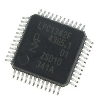
LPC1342FBD48,151 NXP Semiconductors, LPC1342FBD48,151 Datasheet - Page 15

LPC1342FBD48,151
Manufacturer Part Number
LPC1342FBD48,151
Description
IC MCU 32BIT 48LQFP
Manufacturer
NXP Semiconductors
Series
LPC13xxr
Datasheet
1.LPC1342FBD48151.pdf
(62 pages)
Specifications of LPC1342FBD48,151
Core Processor
ARM® Cortex-M3™
Core Size
32-Bit
Speed
72MHz
Connectivity
I²C, Microwire, SPI, SSI, SSP, UART/USART, USB
Peripherals
Brown-out Detect/Reset, POR, WDT
Number Of I /o
40
Program Memory Size
16KB (16K x 8)
Program Memory Type
FLASH
Ram Size
4K x 8
Voltage - Supply (vcc/vdd)
2 V ~ 3.6 V
Data Converters
A/D 8x10b
Oscillator Type
Internal
Operating Temperature
-40°C ~ 85°C
Package / Case
48-LQFP
Processor Series
LPC1342
Core
ARM Cortex-M3
Data Bus Width
32 bit
Data Ram Size
4 KB
Interface Type
I2C, USB, UART
Maximum Clock Frequency
72 MHz
Number Of Programmable I/os
42
Number Of Timers
4
Maximum Operating Temperature
+ 85 C
Mounting Style
SMD/SMT
Minimum Operating Temperature
- 40 C
Lead Free Status / RoHS Status
Lead free / RoHS Compliant
Eeprom Size
-
Lead Free Status / Rohs Status
Details
Other names
568-5214
Available stocks
Company
Part Number
Manufacturer
Quantity
Price
Company:
Part Number:
LPC1342FBD48,151
Manufacturer:
TI
Quantity:
115
Company:
Part Number:
LPC1342FBD48,151
Manufacturer:
NXP Semiconductors
Quantity:
10 000
NXP Semiconductors
Table 4.
[1]
[2]
[3]
[4]
[5]
[6]
[7]
LPC1311_13_42_43
Product data sheet
Symbol
V
XTALIN
XTALOUT
V
DD
SS
Pin state at reset for default function: I = Input; O = Output; PU = internal pull-up enabled; IA = inactive, no pull-up/down enabled.
F = floating; floating pins, if not used, should be tied to ground or power to minimize power consumption.
See
the chip and wake up from Deep power-down mode.
5 V tolerant pad providing digital I/O functions with configurable pull-up/pull-down resistors and configurable hysteresis (see
I
5 V tolerant pad providing digital I/O functions with configurable pull-up/pull-down resistors, configurable hysteresis, and analog input.
When configured as a ADC input, digital section of the pad is disabled, and the pin is not 5 V tolerant (see
Pad provides USB functions. It is designed in accordance with the USB specification, revision 2.0 (Full-speed and Low-speed mode
only).
When the system oscillator is not used, connect XTALIN and XTALOUT as follows: XTALIN can be left floating or can be grounded
(grounding is preferred to reduce susceptibility to noise). XTALOUT should be left floating.
2
C-bus pads compliant with the I
Figure 31
LPC1311/13/42/43 HVQFN33 pin description table
for pad characteristics. RESET functionality is not available in Deep power-down mode. Use the WAKEUP pin to reset
Pin
6;
29
4
5
33
[7]
[7]
Start
logic
input
-
-
-
-
2
C-bus specification for I
Type Reset
I
I
O
-
All information provided in this document is subject to legal disclaimers.
state
[1]
-
-
-
-
Description
3.3 V supply voltage to the internal regulator, the external rail, and the
ADC. Also used as the ADC reference voltage.
Input to the oscillator circuit and internal clock generator circuits. Input
voltage must not exceed 1.8 V.
Output from the oscillator amplifier.
Thermal pad. Connect to ground.
Rev. 3 — 10 August 2010
2
C standard mode and I
…continued
2
C Fast-mode Plus.
32-bit ARM Cortex-M3 microcontroller
LPC1311/13/42/43
Figure
© NXP B.V. 2010. All rights reserved.
30).
Figure
15 of 62
30).


