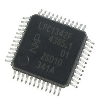
LPC1342FBD48,151 NXP Semiconductors, LPC1342FBD48,151 Datasheet - Page 18

LPC1342FBD48,151
Manufacturer Part Number
LPC1342FBD48,151
Description
IC MCU 32BIT 48LQFP
Manufacturer
NXP Semiconductors
Series
LPC13xxr
Datasheet
1.LPC1342FBD48151.pdf
(62 pages)
Specifications of LPC1342FBD48,151
Core Processor
ARM® Cortex-M3™
Core Size
32-Bit
Speed
72MHz
Connectivity
I²C, Microwire, SPI, SSI, SSP, UART/USART, USB
Peripherals
Brown-out Detect/Reset, POR, WDT
Number Of I /o
40
Program Memory Size
16KB (16K x 8)
Program Memory Type
FLASH
Ram Size
4K x 8
Voltage - Supply (vcc/vdd)
2 V ~ 3.6 V
Data Converters
A/D 8x10b
Oscillator Type
Internal
Operating Temperature
-40°C ~ 85°C
Package / Case
48-LQFP
Processor Series
LPC1342
Core
ARM Cortex-M3
Data Bus Width
32 bit
Data Ram Size
4 KB
Interface Type
I2C, USB, UART
Maximum Clock Frequency
72 MHz
Number Of Programmable I/os
42
Number Of Timers
4
Maximum Operating Temperature
+ 85 C
Mounting Style
SMD/SMT
Minimum Operating Temperature
- 40 C
Lead Free Status / RoHS Status
Lead free / RoHS Compliant
Eeprom Size
-
Lead Free Status / Rohs Status
Details
Other names
568-5214
Available stocks
Company
Part Number
Manufacturer
Quantity
Price
Company:
Part Number:
LPC1342FBD48,151
Manufacturer:
TI
Quantity:
115
Company:
Part Number:
LPC1342FBD48,151
Manufacturer:
NXP Semiconductors
Quantity:
10 000
NXP Semiconductors
LPC1311_13_42_43
Product data sheet
7.6.2 Interrupt sources
7.8.1 Features
7.7 IOCONFIG block
7.8 Fast general purpose parallel I/O
Each peripheral device has one interrupt line connected to the NVIC but may have several
interrupt flags. Individual interrupt flags may also represent more than one interrupt
source.
Any GPIO pin (total of up to 42 pins) regardless of the selected function, can be
programmed to generate an interrupt on a level, or rising edge or falling edge, or both.
The IOCONFIG block allows selected pins of the microcontroller to have more than one
function. Configuration registers control the multiplexers to allow connection between the
pin and the on-chip peripherals.
Peripherals should be connected to the appropriate pins prior to being activated and prior
to any related interrupt(s) being enabled. Activity of any enabled peripheral function that is
not mapped to a related pin should be considered undefined.
Device pins that are not connected to a specific peripheral function are controlled by the
GPIO registers. Pins may be dynamically configured as inputs or outputs. Multiple outputs
can be set or cleared in one write operation.
LPC1311/13/42/43 use accelerated GPIO functions:
Additionally, any GPIO pin (total of up to 42 pins) providing a digital function can be
programmed to generate an interrupt on a level, a rising or falling edge, or both.
•
•
•
•
•
•
•
•
•
8 programmable interrupt priority levels, with hardware priority level masking
Relocatable vector table.
Software interrupt generation.
GPIO block is a dedicated AHB peripheral so that the fastest possible I/O timing can
be achieved.
Entire port value can be written in one instruction.
Bit level port registers allow a single instruction to set or clear any number of bits in
one write operation.
Direction control of individual bits.
All I/O default to inputs with pull-up resistors enabled after reset with the exception of
the I
Pull-up/pull-down resistor configuration can be programmed through the IOCONFIG
block for each GPIO pin.
2
C-bus pins PIO0_4 and PIO0_5.
All information provided in this document is subject to legal disclaimers.
Rev. 3 — 10 August 2010
32-bit ARM Cortex-M3 microcontroller
LPC1311/13/42/43
© NXP B.V. 2010. All rights reserved.
18 of 62


