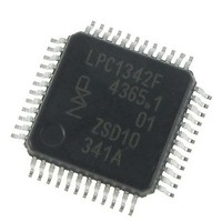
LPC1342FBD48,151 NXP Semiconductors, LPC1342FBD48,151 Datasheet - Page 44

LPC1342FBD48,151
Manufacturer Part Number
LPC1342FBD48,151
Description
IC MCU 32BIT 48LQFP
Manufacturer
NXP Semiconductors
Series
LPC13xxr
Datasheet
1.LPC1342FBD48151.pdf
(62 pages)
Specifications of LPC1342FBD48,151
Core Processor
ARM® Cortex-M3™
Core Size
32-Bit
Speed
72MHz
Connectivity
I²C, Microwire, SPI, SSI, SSP, UART/USART, USB
Peripherals
Brown-out Detect/Reset, POR, WDT
Number Of I /o
40
Program Memory Size
16KB (16K x 8)
Program Memory Type
FLASH
Ram Size
4K x 8
Voltage - Supply (vcc/vdd)
2 V ~ 3.6 V
Data Converters
A/D 8x10b
Oscillator Type
Internal
Operating Temperature
-40°C ~ 85°C
Package / Case
48-LQFP
Processor Series
LPC1342
Core
ARM Cortex-M3
Data Bus Width
32 bit
Data Ram Size
4 KB
Interface Type
I2C, USB, UART
Maximum Clock Frequency
72 MHz
Number Of Programmable I/os
42
Number Of Timers
4
Maximum Operating Temperature
+ 85 C
Mounting Style
SMD/SMT
Minimum Operating Temperature
- 40 C
Lead Free Status / RoHS Status
Lead free / RoHS Compliant
Eeprom Size
-
Lead Free Status / Rohs Status
Details
Other names
568-5214
Available stocks
Company
Part Number
Manufacturer
Quantity
Price
Company:
Part Number:
LPC1342FBD48,151
Manufacturer:
TI
Quantity:
115
Company:
Part Number:
LPC1342FBD48,151
Manufacturer:
NXP Semiconductors
Quantity:
10 000
NXP Semiconductors
Table 15.
T
[1]
Table 16.
T
[1]
[2]
[3]
[4]
[5]
[6]
[7]
LPC1311_13_42_43
Product data sheet
Symbol
f
t
t
t
t
t
Symbol
t
t
SCL
f
LOW
HIGH
HD;DAT
SU;DAT
r
f
amb
amb
Applies to standard port pins and RESET pin.
See the I
Parameters are valid over operating temperature range unless otherwise specified.
t
A device must internally provide a hold time of at least 300 ns for the SDA signal (with respect to the V
bridge the undefined region of the falling edge of SCL.
C
The maximum t
250 ns. This allows series protection resistors to be connected in between the SDA and the SCL pins and the SDA/SCL bus lines
without exceeding the maximum specified t
In Fast-mode Plus, fall time is specified the same for both output stage and bus timing. If series resistors are used, designers should
allow for this when considering bus timing.
HD;DAT
= −40 °C to +85 °C; 3.0 V ≤ V
= −40 °C to +85 °C.
b
= total capacitance of one bus line in pF.
is the data hold time that is measured from the falling edge of SCL; applies to data in transmission and the acknowledge.
Dynamic characteristics: I/O pins
Dynamic characteristic: I
2
C-bus specification UM10204 for details.
10.4 I/O pins
10.5 I
Parameter
SCL clock
frequency
fall time
LOW period of the
SCL clock
HIGH period of the
SCL clock
data hold time
data set-up time
f
Parameter
rise time
fall time
for the SDA and SCL bus lines is specified at 300 ns. The maximum fall time for the SDA output stage t
[2]
2
C-bus
DD
[4][5][6][7]
[3][4][8]
[9][10]
≤ 3.6 V.
2
Conditions
pin configured as output
pin configured as output
C-bus pins
All information provided in this document is subject to legal disclaimers.
f
.
[1]
Conditions
Standard-mode
Fast-mode
Fast-mode Plus
of both SDA and SCL
signals
Standard-mode
Fast-mode
Fast-mode Plus
Standard-mode
Fast-mode
Fast-mode Plus
Standard-mode
Fast-mode
Fast-mode Plus
Standard-mode
Fast-mode
Fast-mode Plus
Rev. 3 — 10 August 2010
[1]
Standard-mode
Fast-mode
Fast-mode Plus
Min
3.0
2.5
Min
0
0
0
-
20 + 0.1 × C
-
4.7
1.3
0.5
4.0
0.6
0.26
0
0
0
250
100
50
32-bit ARM Cortex-M3 microcontroller
LPC1311/13/42/43
b
Typ
-
-
IH
(min) of the SCL signal) to
Max
100
400
1
300
300
120
-
-
-
-
-
-
-
-
-
-
-
-
© NXP B.V. 2010. All rights reserved.
Max
5.0
5.0
f
is specified at
Unit
kHz
kHz
MHz
ns
ns
ns
μs
μs
μs
μs
μs
μs
μs
μs
μs
ns
ns
ns
ns
44 of 62
Unit
ns


