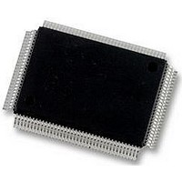
LM97593VH National Semiconductor, LM97593VH Datasheet - Page 25

LM97593VH
Manufacturer Part Number
LM97593VH
Description
12BIT ADC, 2CH, DDC/AGC, 128PQFP
Manufacturer
National Semiconductor
Datasheet
1.LM97593VH.pdf
(50 pages)
Specifications of LM97593VH
Resolution (bits)
12bit
Input Channel Type
Differential
Data Interface
Serial
Supply Voltage Range - Analogue
3V To 3.6V
Supply Voltage Range - Digital
1.6V To 2V, 3V To 3.6V
Supply
RoHS Compliant
Sampling Rate
65MSPS
Rohs Compliant
Yes
Lead Free Status / Rohs Status
Not Compliant
Available stocks
Company
Part Number
Manufacturer
Quantity
Price
Company:
Part Number:
LM97593VH/NOPB
Manufacturer:
VK
Quantity:
1 980
Company:
Part Number:
LM97593VH/NOPB
Manufacturer:
Texas Instruments
Quantity:
10 000
control port. Page select bits allow access to the overlaid A
and B set of FIR coefficients.
JTAG boundary scan and on-chip diagnostic circuits are pro-
vided to simplify system debug and test.
The LM97593 supports 3.3V I/O even though the core logic
voltage is 1.8V. The LM97593 outputs swing to the 3.3V rail
so they can be directly connected to 5V TTL inputs if desired.
ADC Application Information
1.0 ADC OPERATING CONDITIONS
We recommend that the following conditions be observed for
operation:
1.1 Analog Inputs
There is one reference input pin, V
an internal reference, or to supply an external reference. The
ADC has two analog signal input pairs, V
one converter and V
Each pair of pins forms a differential input pair.
1.2 Reference Pins
The ADC is designed to operate with an internal 1.0V refer-
ence or an external 1.0V reference, but performs well with
external reference voltages in the range of 0.8V to 1.2V. Low-
er reference voltages will decrease the signal-to-noise ratio
(SNR) of the ADC. Increasing the reference voltage (and the
input signal swing) beyond 1.2V may degrade THD for a full-
scale input, especially at higher input frequencies.
It is important that all grounds associated with the reference
voltage and the analog input signal make connection to the
ground plane at a single, quiet point to minimize the effects of
noise currents in the ground path.
The six Reference Bypass Pins (V
V
All these pins should each be bypassed to ground with a 0.1
µF capacitor. A 10 µF capacitor should be placed between the
V
as shown in Figure 45. This configuration is necessary to
avoid reference oscillation, which could result in reduced
SFDR and/or SNR.
Smaller capacitor values than those specified will allow faster
recovery from the power down mode, but may result in de-
graded noise performance. Loading any of these pins other
than V
tion.
The nominal voltages for the reference bypass pins are as
follows:
User choice of an on-chip or external reference voltage is
provided. The internal 1.0 Volt reference is in use when the
the V
0.8V to 1.2V is applied to the V
voltage reference. When an external reference is used, the
V
COM
RP
REF
3.0V
V
V
10 MHz
1.0 V internal reference
V
V
V
V
D
D18
A and V
COM
RP
RN
CM
pin should be bypassed to ground with a 0.1 µF capacitor
B and V
REF
= V
COM
= V
= V
= 1.8V
≤
= 1.5V (from V
= 1.5 V
A
pin is connected to V
V
COM
COM
A and V
= V
≤
A
RN
f
≤
CLK
RN
DR
A pins and between the V
+ V
− V
3.6V
B) are made available for bypass purposes.
≤
REF
REF
COM
65 MHz
IN
/ 2
/ 2
COM
B may result in performance degrada-
B+ and V
A and V
A
IN
. If a voltage in the range of
REF
REF
COM
B- for the other converter.
RP
pin, that is used for the
A, V
, which is used to select
B)
RP
IN
COM
B and V
A+ and V
A, V
RN
RN
A, V
IN
B pins,
A- for
RP
B,
25
close to the reference input pin. There is no need to bypass
the V
1.3 Signal Inputs
The signal inputs are V
V
defined as
for the "A" converter and
for the "B" converter. Figure 17 shows the expected input sig-
nal range. Note that the common mode input voltage, V
should be in the range of 1.0V to 2.0V.
The peaks of the individual input signals should never exceed
2.6V.
The ADC performs best with a differential input signal with
each input centered around a common mode voltage, V
The peak-to-peak voltage swing at each analog input pin
should not exceed the value of the reference voltage or the
output data will be clipped.
The two input signals should be exactly 180° out of phase
from each other and of the same amplitude. For single fre-
quency inputs, angular errors result in a reduction of the
effective full scale input. For complex waveforms, however,
angular errors will result in distortion.
For single frequency sine waves the full scale error in LSBs
can be described as approximately
E
Where dev is the angular difference in degrees between the
two signals having a 180° relative phase relationship to each
other (see Figure 18). Drive the analog inputs with a source
impedance less than 100Ω.
Signals Will Reduce the Output Level or Cause Distortion
For differential operation, each analog input pin of the differ-
ential pair should have a peak-to-peak voltage equal to the
IN
FS
V
V
FIGURE 18. Angular Errors Between the Two Input
B+ and V
= 4096 ( 1 - sin (90° + dev))
IN
IN
REF
A = (V
B = (V
FIGURE 17. Expected Input Signal Range
pin when the internal reference is used.
IN
IN
IN
B− for the other ADC . The input signal, V
A+) – (V
B+) – (V
IN
IN
IN
A−)
B−)
A+ and V
IN
30008751
A− for one ADC and
30008750
www.national.com
(Eq. 1)
(Eq. 2)
(Eq. 3)
IN
CM
CM
, is
,
.


