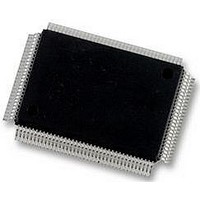
LM97593VH National Semiconductor, LM97593VH Datasheet - Page 43

LM97593VH
Manufacturer Part Number
LM97593VH
Description
12BIT ADC, 2CH, DDC/AGC, 128PQFP
Manufacturer
National Semiconductor
Datasheet
1.LM97593VH.pdf
(50 pages)
Specifications of LM97593VH
Resolution (bits)
12bit
Input Channel Type
Differential
Data Interface
Serial
Supply Voltage Range - Analogue
3V To 3.6V
Supply Voltage Range - Digital
1.6V To 2V, 3V To 3.6V
Supply
RoHS Compliant
Sampling Rate
65MSPS
Rohs Compliant
Yes
Lead Free Status / Rohs Status
Not Compliant
Available stocks
Company
Part Number
Manufacturer
Quantity
Price
Company:
Part Number:
LM97593VH/NOPB
Manufacturer:
VK
Quantity:
1 980
Company:
Part Number:
LM97593VH/NOPB
Manufacturer:
Texas Instruments
Quantity:
10 000
000 = -12dB
001 = -6dB
010 = 0dB
011 = +6dB
100 = +12dB
101 = +18dB
110 = +24dB
111 = +30dB
These values are shown with respect to the table addresses
in Figure 42, and the CIC filter output P
a 52MHz clock rate and AGC_LOOP_GAIN=2, these values
result in a loop time constant of 1.5µs.
The error signal from the loop gain “SHIFT DOWN” circuit is
gated into the loop integrator. A MUX within the integrator
feedback allows the integrator to be initialized to the value
loaded into AGC_IC_A (channel B can be set independently).
The top eight bits of the integrator output can also be read
back over the microprocessor interface from the AGC_RB_A
(or AGC_RB_B) register. The top 3 bits become AGAIN and
are output along with the ASTROBE signal on the DVGA in-
terface pins. The valid range of AGAIN is from 0 to 7 which
corresponds to a valid range of 0 to 2
complement integrator output from which AGAIN is derived.
This is illustrated in Figure 44. The integrator saturates at
these limits to prevent overshoots as the integrator attempts
to enter the valid range. The AGAIN value is inverted (EXP)
AGAIN
FIGURE 42. Example of programmed RAM contents
a. AGAIN sets the DVGA or analog gain value.
b. EXP sets the "FIXED TO FLOAT CONVERTER" or digital gain value.
c. 22-bit input to SHIFT-UP block in Figure 19 horizontally, linearized SHIFT-UP value vertically.
d. The numbers in the center of the table represent the mixer output bits. 'L' represents a logic low.
a
111 = +0dB
110 = -6dB
101 = -12dB
100 = -18dB
011 = -24dB
010 = -30dB
001 = -36dB
000 = -42dB
EXP
TABLE 5. 15-bit Mixer Output Alignment into the 22-bit SHIFT-UP Based On EXP
b
Input
-12dB
-12dB
-12dB
-12dB
-12dB
-12dB
-12dB
-12dB
c
11
OUT
-1 for the 11-bit, 2’s
in Figure 43. For
21
14
14
14
14
14
14
14
14
d
30008739
20 19 18 17 16 15 14
13 12 11 10
14 13 12 11 10
14 14 13 12 11 10
14 14 14 13 12 11 10
14 14 14 14 13 12 11
14 14 14 14 14 13 12
14 14 14 14 14 14 13
14 14 14 14 14 14 14
43
and used to adjust the gain of the incoming signal to provide
a linear output dynamic range. The relationship between the
DVGA analog gain (AGAIN) and the “FIXED TO FLOAT
CONVERTER” digital gain (EXP) is shown in Table 5. The
DVGA’s compression of the incoming signal in the analog
domain vs. the subsequent expansion in the digital domain is
shown in Figure 36.
The AGC may be forced to free run by setting AGC_HOLD_IC
low. Writing an initial condition to AGC_IC_A|B and then set-
ting AGC_HOLD_IC high will force the AGC to a fixed gain.
The three MSBs of the value written to AGC_IC_A|B are in-
verted and output to drive the DVGA.
Allowing the AGC to free run should be appropriate for most
applications. If the INH_EXP bit is not set, the DVGA gain
word (EXP) is routed to the “FLOAT TO FIXED CONVERT-
ER” in the DDCs prior to the programmable decimation filter.
The EXP signals are delayed to account for the propagation
delay of the DVGA interface and the ADC12DL080 ADC.
9
FIGURE 43. Example of programmed RAM contents
8
9
7
8
9
...
...
...
...
...
...
...
...
...
8
1
2
3
4
5
6
7
8
7
0
1
2
3
4
5
6
7
6
L
0
1
2
3
4
5
6
5
L
L
0
1
2
3
4
5
4
L
L
L
0
1
2
3
4
3
L
L
L
L
0
1
2
3
30008740
www.national.com
2
L
L
L
L
L
0
1
2
1
L
L
L
L
L
L
0
1
0
L
L
L
L
L
L
L
0


