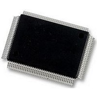
LM97593VH National Semiconductor, LM97593VH Datasheet - Page 39

LM97593VH
Manufacturer Part Number
LM97593VH
Description
12BIT ADC, 2CH, DDC/AGC, 128PQFP
Manufacturer
National Semiconductor
Datasheet
1.LM97593VH.pdf
(50 pages)
Specifications of LM97593VH
Resolution (bits)
12bit
Input Channel Type
Differential
Data Interface
Serial
Supply Voltage Range - Analogue
3V To 3.6V
Supply Voltage Range - Digital
1.6V To 2V, 3V To 3.6V
Supply
RoHS Compliant
Sampling Rate
65MSPS
Rohs Compliant
Yes
Lead Free Status / Rohs Status
Not Compliant
Available stocks
Company
Part Number
Manufacturer
Quantity
Price
Company:
Part Number:
LM97593VH/NOPB
Manufacturer:
VK
Quantity:
1 980
Company:
Part Number:
LM97593VH/NOPB
Manufacturer:
Texas Instruments
Quantity:
10 000
COEF_SEL_F1A
COEF_SEL_F1B
PAGE_SEL_F1
COEF_SEL_F2A
COEF_SEL_F2B
PAGE_SEL_F2
SFS_MODE
SDC_EN
AGC_COMB_ORD
EXT_DELAY
DEC
DEC_BY_4
SCALE
GAIN_A
GAIN_B
RATE
SERIAL_CTRL
FREQ_A
PHASE_A
FREQ_B
PHASE_B
Source
AGC_CTRL
AGC_COUNT
9.2 Condensed LM97593 Address Map
Register Name
Register Name
Register
Name
a. These are the default values set by a master reset (MR). Sync in (SI) will not affect any of these values.
Addr
10
11
12
13
14
15
16
17
18
19
20
21
22
0
1
2
3
4
5
6
7
8
9
Width
Width
1b
1b
1b
1b
1b
1b
1b
1b
2b
5b
Addr
0x0C
0x0D
0x0A
0x0B
0x0E
0x0F
0x00
0x01
0x02
0x03
0x04
0x05
0x06
0x07
0x08
0x09
0x10
0x11
0x12
0x13
0x14
0x15
0x16
Hex
Type
Type
R/W
R/W
R/W
R/W
R/W
R/W
R/W
R/W
R/W
R/W
Reserved
Reserved
Rate7
FMT1
FA15
FA23
FA31
PA15
FB15
FB23
FB31
PB15
Dec7
Bit7
FA7
PA7
FB7
PB7
Default
Default
0
0
0
0
0
0
0
0
0
0
Reserved Reserved Reserved Reserved Reserved Reserved Reserved
Reserved Reserved Reserved Reserved Reserved Reserved Reserved
a
a
Rate6
FMT0
Dec6
FA14
FA22
FA30
PA14
FB14
FB22
FB30
PB14
Bit6
FA6
PA6
FB6
PB6
Addr
Addr
246
246
246
247
247
247
248
248
249
249
AgcLG1
Packed
Rate5
PA13
PB13
Dec5
FA13
FA21
FA29
FB13
FB21
FB29
Bit5
PA5
PB5
FA5
FB5
Sc5
1:0
6:2
Bit
Bit
0
1
2
0
1
2
0
1
39
Channel A F1 coefficient select register. 0=memory A,
1=memory B.
Channel B F1 coefficient select register. 0=memory A,
1=memory B.
F1 coefficient page select register. 0=memory A, 1=memory B.
Channel A F2 coefficient select register. 0=memory A,
1=memory B.
Channel B F2 coefficient select register. 0=memory A,
1=memory B.
F2 coefficient page select register. 0=memory A, 1=memory B.
0=SFS asserted at the start of each output word when
PACKED=1 or each I/Q pair when PACKED=0, 1=SFS asserted
at the start of each output sample period.
0=normal serial mode, 1=serial daisy-chain master mode.
Enable reduced bandwidth AGC power detector. 0=2
decimate-by-eight CIC, 1=1-tap comb added to CIC, 2=4-tap
comb added to CIC.
Number of CK period delays needed to align the DVGA gain
step with the digital gain compensation step. Set this register to
7 if ASTROBE and BSTROBE are not used. Otherwise set to 8.
Dec4
DecBy4
Sc4
Rate4
MuxMode RDY_POL SFS_POL SCK_POL SOUT_EN
FA4
FA12
FA20
FA28
PA4
PA12
FB4
FB12
FB20
FB28
PB4
PB12
AgcLG0
Bit4
Dec3
Sc3
Rate3
FA3
FA11
FA19
FA27
PA3
PA11
FB3
FB11
FB19
FB27
PB3
PB11
BS1
AgcHldlC
Bit3
Dec2
Dec10
Sc2
GA2
GB2
Rate2
FA2
FA10
FA18
FA26
PA2
PA10
FB2
FB10
FB18
FB26
PB2
PB10
BS0
Reserved Reserved Explnh
Description
Description
Bit2
Dec1
Dec9
Sc1
GA1
GB1
Rate1
FA1
FA9
FA17
FA25
PA1
PA9
FB1
FB9
FB17
FB25
PB1
PB9
AS1
Bit1
Dec0
Dec8
Sc0
GA0
GB0
Rate0
FA0
FA8
FA16
FA24
PA0
PA8
FB0
FB8
FB16
FB24
PB0
PB8
AS0
www.national.com
nd
Bit0
-order


