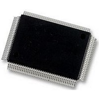
LM97593VH National Semiconductor, LM97593VH Datasheet - Page 36

LM97593VH
Manufacturer Part Number
LM97593VH
Description
12BIT ADC, 2CH, DDC/AGC, 128PQFP
Manufacturer
National Semiconductor
Datasheet
1.LM97593VH.pdf
(50 pages)
Specifications of LM97593VH
Resolution (bits)
12bit
Input Channel Type
Differential
Data Interface
Serial
Supply Voltage Range - Analogue
3V To 3.6V
Supply Voltage Range - Digital
1.6V To 2V, 3V To 3.6V
Supply
RoHS Compliant
Sampling Rate
65MSPS
Rohs Compliant
Yes
Lead Free Status / Rohs Status
Not Compliant
Available stocks
Company
Part Number
Manufacturer
Quantity
Price
Company:
Part Number:
LM97593VH/NOPB
Manufacturer:
VK
Quantity:
1 980
Company:
Part Number:
LM97593VH/NOPB
Manufacturer:
Texas Instruments
Quantity:
10 000
www.national.com
DEC
DEC_BY_4
SCALE
GAIN_A
GAIN_B
RATE
SOUT_EN
SCK_POL
7.0 POWER MANAGEMENT
The LM97593 can be placed in a low power (static) state by
stopping the input clock and setting the PD pin high. To pre-
vent this from placing the LM97593 into unexpected states,
the SI pin of the LM97593 should be asserted prior to dis-
abling the input clock and held asserted until the input clock
has returned to a stable condition.
8.0 TESTABILITY
8.1 JTAG Boundary Scan
The LM97593 supports IEEE 1149.1 compliant JTAG Bound-
ary Scan for the I/O's. The following pins are used:
The following JTAG instructions are supported:
The JTAG Boundary Scan can be used to verify printed circuit
board continuity at the system level.
8.2 Test Register
The user is able to program a value into TEST_REG and
substitute this for the normal channel inputs from the AIN/
BIN pins by selecting it with the crossbar. With the NCO fre-
quency set to zero this allows the DDCs and the output
9.1 Control Register Addresses and Defaults
Register Name
Instruction
BYPASS
EXTEST
IDCODE
SAMPLE/PRELOAD
HIGHZ
TRST (test reset)
TMS
TDI
TDO
TCK
(test mode select)
(test data in)
(test data out)
(test clock)
Width
11b
1B
1b
6b
3b
3b
1b
1b
Description
Connects TDI directly to TDO
Enables the test access port
controller to drive the outputs
Connects the 32-bit ID register to
TDO
Allows the test access port to
sample the device inputs and
preload test output data
Tri-states the outputs
Type
R/W
R/W
R/W
R/W
R/W
R/W
R/W
R/W
Default
7
0
0
0
0
1
0
0
a
1(MSBs)
0(LSBs)
Addr
1
2
3
4
5
6
6
Bit
7:0
2:0
5:0
2:0
2:0
7:0
4
0
1
36
CIC decimation control. N=DEC+1. Valid range is from 7 to
2047. Format is an unsigned integer. This affects both channels.
Controls the decimation factor in F2. 0=Decimate by 2.
1=Decimate by 4. This affects both channels.
CIC SCALE parameter. Format is an unsigned integer
representing the number of left bit shifts to perform on the data
prior to the CIC filter. Valid range is from 0 to 40. This affects
both channels.
Value of left bit shift prior to F1 for channel A.
Value of left bit shift prior to F1 for channel B.
Determines rate of serial output clock. The output rate is FCK/
(RATE+1). Unsigned integer values of 0, 1, 3, 7, 15, and 31 are
allowed.
Enables the serial output pins AOUT, BOUT, SCK, and SFS.
0=Tristate. 1=Enabled.
Determines polarity of the SCK output. 0=AOUT, BOUT, and
SFS change on the rising edge of SCK (capture on falling edge).
1=They change on the falling edge of SCK.
interface of the chip to be verified. Also, the AGC loop can be
opened by setting AGC_HOLD_IC high and setting the gain
of the DVGA by programming the appropriate value into the
AGC_IC_A/B register.
8.3 Debug Access Port
Real-time access to the following signals is provided by con-
figuring the control interface debug register:
•
•
•
•
The access points are multiplexed to a 20-bit parallel output
port which is created from signal pins POUT[15:0], AOUT,
BOUT, SFS, and RDY according to the table below:
SCK will be set to the proper strobe rate for each debug tap
point. POUT_EN and PSEL[2:0] have no effect in Debug
Mode. The outputs are turned on when the Debug Mode bit
is set. Normal serial outputs are also disabled.
9.0 CONTROL REGISTERS
The chip is configured and controlled through the use of 8-bit
control registers. These registers are accessed for reading or
writing using the control bus pins (CE, RD, WR, A[7:0], and D
[7:0]) described in section 3.0 Control Interface.
The two sets of FIR coefficients are overlaid at the same
memory address. Use the PAGE_SEL registers to access
the second set of coefficients.
The register names and descriptions are listed below in sec-
tion 9.1 Control Register Addresses and Defaults. A quick
reference table is provided in the Condensed LM97593 Ad-
dress Map.
NCO sine and cosine outputs
data after round following mixers
data before F1 and F2
data after CIC filter within the AGC
Normal Mode Pin
POUT[15:0]
RDY
SFS
AOUT
BOUT
Description
Debug Mode Pin
DEBUG[19:4]
DEBUG[3]
DEBUG[2]
DEBUG[1]
DEBUG[0]


