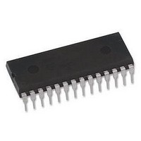
DSPIC30F2010-30I/SPG Microchip Technology, DSPIC30F2010-30I/SPG Datasheet - Page 57

DSPIC30F2010-30I/SPG
Manufacturer Part Number
DSPIC30F2010-30I/SPG
Description
16BIT 30MIPS DSPIC, 30F2010, DIP28
Manufacturer
Microchip Technology
Series
DsPIC30Fr
Datasheet
1.DSPIC30F2010-30ISPG.pdf
(244 pages)
Specifications of DSPIC30F2010-30I/SPG
Core Frequency
30MHz
Embedded Interface Type
I2C, SPI, UART
No. Of I/o's
20
Flash Memory Size
12KB
Supply Voltage Range
2.5V To 5.5V
Operating Temperature Range
-40°C To
Lead Free Status / RoHS Status
Lead free / RoHS Compliant
- Current page: 57 of 244
- Download datasheet (7Mb)
6.0
The dsPIC30F family of devices contains internal
program Flash memory for executing user code. There
are two methods by which the user can program this
memory:
1.
2.
6.1
dsPIC30F devices can be serially programmed while in
the end application circuit. This is simply done with two
lines for Programming Clock and Programming Data
(which are named PGC and PGD respectively), and
three other lines for Power (V
Master Clear (MCLR). this allows customers to manu-
facture boards with unprogrammed devices, and then
program the microcontroller just before shipping the
product. This also allows the most recent firmware or a
custom firmware to be programmed.
FIGURE 6-1:
2004 Microchip Technology Inc.
Note: This data sheet summarizes the features of this family of dsPIC30F devices and is not intended to be a complete reference
source. For complete information on the CPU, peripherals, register descriptions and general device functionality, please refer to the
dsPIC30F Family Reference Manual (DS70046). For complete information on the device instruction set and programming, please
refer to the dsPIC30F Programmer’s Reference Manual (DS70030). For device pinouts and electrical specifications, please refer to
the specific data sheet for the device that will be used in your design.
In-Circuit Serial Programming
Run Time Self-Programming (RTSP)
User/Configuration
Space Select
FLASH PROGRAM MEMORY
In-Circuit Serial Programming
(ICSP)
ADDRESSING FOR TABLE AND NVM REGISTERS
Using
NVMADR
Addressing
Using
Table
Instruction
Using
Program
Counter
DD
), Ground (V
TM
(ICSP
1/0
1/0
0
TM
Advance Information
TBLPAG Reg
NVMADRU Reg
)
SS
8 bits
8 bits
) and
Program Counter
24 bits
24-bit EA
6.2
RTSP is accomplished using TBLRD (table read) and
TBLWT (table write) instructions.
With RTSP, the user may erase and program 32
instructions (96 bytes) at a time.
6.3
The TBLRDL and the TBLWTL instructions are used to
read or write to bits <15:0> of program memory.
TBLRDL and TBLWTL can access program memory in
Word or Byte mode.
The TBLRDH and TBLWTH instructions are used to read
or write to bits<23:16> of program memory. TBLRDH
and TBLWTH can access program memory in Word or
Byte mode.
A 24-bit program memory address is formed using
bits<7:0> of the TBLPAG register and the effective
address (EA) from a W register specified in the table
instruction, as shown in Figure 6-1.
NVMADR Reg EA
Working Reg EA
16 bits
16 bits
Run Time Self-Programming
(RTSP)
Table Instruction Operation Summary
0
Byte
Select
dsPIC30F
DS70082E-page 55
Related parts for DSPIC30F2010-30I/SPG
Image
Part Number
Description
Manufacturer
Datasheet
Request
R

Part Number:
Description:
IC DSPIC MCU/DSP 12K 28DIP
Manufacturer:
Microchip Technology
Datasheet:

Part Number:
Description:
IC DSPIC MCU/DSP 12K 28SOIC
Manufacturer:
Microchip Technology
Datasheet:

Part Number:
Description:
IC,DSP,16-BIT,CMOS,SOP,28PIN,PLASTIC
Manufacturer:
Microchip Technology
Datasheet:

Part Number:
Description:
IC DSPIC MCU/DSP 12K 28SOIC
Manufacturer:
Microchip Technology
Datasheet:

Part Number:
Description:
IC DSPIC MCU/DSP 12K 28QFN
Manufacturer:
Microchip Technology
Datasheet:

Part Number:
Description:
IC DSPIC MCU/DSP 12K 28QFN
Manufacturer:
Microchip Technology
Datasheet:

Part Number:
Description:
IC DSPIC MCU/DSP 12K 28DIP
Manufacturer:
Microchip Technology
Datasheet:

Part Number:
Description:
IC DSPIC MCU/DSP 12K 28SOIC
Manufacturer:
Microchip Technology
Datasheet:

Part Number:
Description:
IC DSPIC MCU/DSP 12K 28DIP
Manufacturer:
Microchip Technology
Datasheet:

Part Number:
Description:
IC DSPIC MCU/DSP 12K 28SOIC
Manufacturer:
Microchip Technology

Part Number:
Description:
IC DSPIC MCU/DSP 12K 28QFN
Manufacturer:
Microchip Technology

Part Number:
Description:
IC DSPIC MCU/DSP 12K 28DIP
Manufacturer:
Microchip Technology

Part Number:
Description:
IC,DSP,16-BIT,CMOS,LLCC,28PIN,PLASTIC
Manufacturer:
Microchip Technology
Datasheet:

Part Number:
Description:
Digital Signal Processors & Controllers - DSP, DSC
Manufacturer:
Microchip Technology

Part Number:
Description:
Digital Signal Processors & Controllers - DSP, DSC 16 Bit MCU/DSP 28LD 20M 12KB FL
Manufacturer:
Microchip Technology


