PIC24FJ256GA106-I/MR Microchip Technology, PIC24FJ256GA106-I/MR Datasheet - Page 15
PIC24FJ256GA106-I/MR
Manufacturer Part Number
PIC24FJ256GA106-I/MR
Description
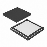
IC, 16BIT MCU, PIC24F, 32MHZ, QFN-64
Manufacturer
Microchip Technology
Series
PIC® 24Fr
Datasheets
1.PIC24FJ128GA008-IPT.pdf
(12 pages)
2.PIC24FJ128GA106-IPT.pdf
(14 pages)
3.PIC24FJ128GA106-IPT.pdf
(330 pages)
4.PIC24FJ128GA106-IPT.pdf
(52 pages)
5.PIC24FJ256GA106-IPT.pdf
(59 pages)
6.PIC24FJ128GB110-IPF.pdf
(292 pages)
Specifications of PIC24FJ256GA106-I/MR
Controller Family/series
PIC24
No. Of I/o's
53
Ram Memory Size
16KB
Cpu Speed
32MHz
No. Of Timers
5
Core Size
16 Bit
Program Memory Size
256KB
Peripherals
ADC, Comparator, PWM, RTC, Timer
Core Processor
PIC
Speed
32MHz
Connectivity
I²C, PMP, SPI, UART/USART
Number Of I /o
53
Program Memory Type
FLASH
Ram Size
16K x 8
Voltage - Supply (vcc/vdd)
2 V ~ 3.6 V
Data Converters
A/D 16x10b
Oscillator Type
Internal
Operating Temperature
-40°C ~ 85°C
Package / Case
64-VFQFN, Exposed Pad
Processor Series
PIC24FJ
Core
PIC
Data Bus Width
16 bit
Data Ram Size
16 KB
Interface Type
I2C, SPI, UART
Maximum Clock Frequency
32 MHz
Number Of Programmable I/os
52
Number Of Timers
5
Maximum Operating Temperature
+ 85 C
Mounting Style
SMD/SMT
3rd Party Development Tools
52713-733, 52714-737, 53276-922, EWDSPIC
Development Tools By Supplier
PG164130, DV164035, DV244005, DV164005, PG164120, DM240001, DM240011
Minimum Operating Temperature
- 40 C
On-chip Adc
10 bit, 16 Channel
Lead Free Status / RoHS Status
Lead free / RoHS Compliant
For Use With
876-1004 - PIC24 BREAKOUT BOARD
Eeprom Size
-
Lead Free Status / Rohs Status
Details


3.2.1
The SIX control code allows execution of PIC24F family
assembly instructions. When the SIX code is received,
the CPU is suspended for 24 clock cycles, as the instruc-
tion is then clocked into the internal buffer. Once the
instruction is shifted in, the state machine allows it to be
executed over the next four PGECx clock cycles. While
the received instruction is executed, the state machine
simultaneously shifts in the next 4-bit command (see
Figure
FIGURE 3-2:
3.2.1.1
There are some important differences between
executing instructions normally and using the SIX ICSP
command. Therefore, the code examples in this speci-
fication may not match those for performing the same
functions during normal device operation.
During SIX ICSP operation:
• Two-word instructions require two SIX operations
• Two-cycle instructions require two SIX operations.
• The CPU does not automatically stall to account
2010 Microchip Technology Inc.
PGECx
PGEDx
to clock in all the necessary data.
Examples of two-word instructions are GOTO and
CALL.
The first SIX operation shifts in the instruction and
begins to execute it. The second SIX operation,
which should shift in a NOP to avoid losing data,
provides the CPU clocks required to finish
executing the instruction.
Examples of two-cycle instructions are Table Read
and Table Write instructions.
for pipeline changes.
A CPU stall occurs when an instruction modifies a
register that is used for indirect addressing by the
following instruction.
P2
0
1
Execute PC – 1,
3-2).
Control Code
Fetch SIX
0
2
SIX SERIAL INSTRUCTION
EXECUTION
P3
0
Differences Between the Execution
of SIX and Normal Instructions
3
0
4
0
5
SIX SERIAL EXECUTION
Memory Entry
0
6
Program
Only for
0
7
0
8
PIC24FJXXXDA1/DA2/GB2/GA3
0
9
P4
LSB X
1
2
P1B
X
P1A
3
X
4
P1
PGEDx = Input
X
5
X
24-Bit Instruction Fetch
6
X
Coming out of Reset, the first 4-bit control code is
always forced to SIX and a forced NOP instruction is
executed by the CPU. Five additional PGECx clocks
are needed on start-up, resulting in a 9-bit SIX
command instead of the normal 4-bit SIX command.
After the forced SIX is clocked in, ICSP operation
resumes as normal. That is, the next 24 clock cycles
load the first instruction word to the CPU.
During normal device operation:
• The CPU automatically will force a NOP while the new
• The device Program Counter (PC) continues to
Note:
data is read. When using ICSP, there is no automatic
stall, so any indirect references to a recently modified
register should be preceded by a NOP.
For example, the instructions, MOV #0x0,W0 and
MOV [W0],W1, must have a NOP inserted among
them.
If a two-cycle instruction modifies a register that is
used indirectly, it will require two NOPs: one to
execute the second half of the instruction and the
other to stall the CPU to correct the pipeline.
Instructions, such as TBLWTL [W0++],[W1],
should be followed by two NOPs.
automatically increment during ICSP instruction
execution, even though the Flash memory is not
being used.
As a result, the PC may be incremented to point to
invalid memory locations. Invalid memory spaces
include unimplemented Flash addresses and the
vector space (locations: 0x0 to 0x1FF).
If the PC points to these locations, the device will
reset, possibly interrupting the ICSP operation. To
prevent this, instructions should be periodically
executed to reset the PC to a safe space. The
optimal method to accomplish this is to perform a
GOTO 0x200.
7
X
8
X
17
X
To account for this forced NOP, all example
code in this specification begins with a
NOP to ensure that no data is lost.
18 19 20 21 22
X
X
X
X
X MSB
23 24
DS39970B-page 15
P4A
Next Control Code
Instruction, Fetch
0
Execute 24-Bit
1
0
2
0
3
0
4
Related parts for PIC24FJ256GA106-I/MR
Image
Part Number
Description
Manufacturer
Datasheet
Request
R

Part Number:
Description:
Manufacturer:
Microchip Technology Inc.
Datasheet:
Part Number:
Description:
Manufacturer:
Microchip Technology Inc.
Datasheet:
Part Number:
Description:
Manufacturer:
Microchip Technology Inc.
Datasheet:
Part Number:
Description:
Manufacturer:
Microchip Technology Inc.
Datasheet:
Part Number:
Description:
Manufacturer:
Microchip Technology Inc.
Datasheet:
Part Number:
Description:
Manufacturer:
Microchip Technology Inc.
Datasheet:
Part Number:
Description:
Manufacturer:
Microchip Technology Inc.
Datasheet:
Part Number:
Description:
Manufacturer:
Microchip Technology Inc.
Datasheet: