PIC24FJ256GA106-I/MR Microchip Technology, PIC24FJ256GA106-I/MR Datasheet - Page 35
PIC24FJ256GA106-I/MR
Manufacturer Part Number
PIC24FJ256GA106-I/MR
Description
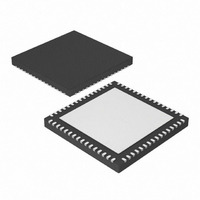
IC, 16BIT MCU, PIC24F, 32MHZ, QFN-64
Manufacturer
Microchip Technology
Series
PIC® 24Fr
Datasheets
1.PIC24FJ128GA008-IPT.pdf
(12 pages)
2.PIC24FJ128GA106-IPT.pdf
(14 pages)
3.PIC24FJ128GA106-IPT.pdf
(330 pages)
4.PIC24FJ128GA106-IPT.pdf
(52 pages)
5.PIC24FJ256GA106-IPT.pdf
(59 pages)
6.PIC24FJ128GB110-IPF.pdf
(292 pages)
Specifications of PIC24FJ256GA106-I/MR
Controller Family/series
PIC24
No. Of I/o's
53
Ram Memory Size
16KB
Cpu Speed
32MHz
No. Of Timers
5
Core Size
16 Bit
Program Memory Size
256KB
Peripherals
ADC, Comparator, PWM, RTC, Timer
Core Processor
PIC
Speed
32MHz
Connectivity
I²C, PMP, SPI, UART/USART
Number Of I /o
53
Program Memory Type
FLASH
Ram Size
16K x 8
Voltage - Supply (vcc/vdd)
2 V ~ 3.6 V
Data Converters
A/D 16x10b
Oscillator Type
Internal
Operating Temperature
-40°C ~ 85°C
Package / Case
64-VFQFN, Exposed Pad
Processor Series
PIC24FJ
Core
PIC
Data Bus Width
16 bit
Data Ram Size
16 KB
Interface Type
I2C, SPI, UART
Maximum Clock Frequency
32 MHz
Number Of Programmable I/os
52
Number Of Timers
5
Maximum Operating Temperature
+ 85 C
Mounting Style
SMD/SMT
3rd Party Development Tools
52713-733, 52714-737, 53276-922, EWDSPIC
Development Tools By Supplier
PG164130, DV164035, DV244005, DV164005, PG164120, DM240001, DM240011
Minimum Operating Temperature
- 40 C
On-chip Adc
10 bit, 16 Channel
Lead Free Status / RoHS Status
Lead free / RoHS Compliant
For Use With
876-1004 - PIC24 BREAKOUT BOARD
Eeprom Size
-
Lead Free Status / Rohs Status
Details


Table 4-3
PIC24FJXXXGA3 Configuration bits in the Flash
Configuration Words.
TABLE 4-3:
2010 Microchip Technology Inc.
ALTVREF<1:0>
BBEN
BBDIS
BOREN
BORV
DEBUG
DSBITEN
DSWDTEN
DSBOREN
DSWDTOSC
Note 1:
Note:
2:
3:
Bit Field
Bits<23:16> should be programmed to a value of 0x00 to ensure that accidental program execution of any
of the Configuration Words would be interpreted as a NOP opcode.
The JTAGEN bit can be modified only using In-Circuit Serial Programming™ (ICSP™).
Irrespective of the WPCFG status, if WPEND = 1 or if WPFP corresponds to the Configuration Words
page, the Configuration Words page will be protected
Although not implemented with a specific
function, the bit at CW1<15> must always
be maintained as ‘0’ to ensure device
functionality, regardless of the settings of
other Configuration bits.
provides
PIC24FJXXXGA3 CONFIGURATION BITS DESCRIPTION
the
CW2<12:11> Alternate V
Register
descriptions
CW4<10>
CW3<12>
CW1<11>
CW2<2>
CW2<3>
CW4<8>
CW4<7>
CW4<6>
CW4<5>
PIC24FJXXXDA1/DA2/GB2/GA3
(1)
00 = AV
01 = AV
10 = AV
11 = AV
Back Bias Enable bit
0 = Back bias is disabled
1 = Back bias is enabled
Back Bias Feature Disable bit
0 = Back bias feature enabled in Deep Sleep
1 = Back bias feature disabled
Brown-out Reset Enable bit
0 = BORMV is disabled
1 = BORMV is enabled outside of Deep Sleep (BORMV is always
Brown-out Reset Voltage bit
0 = BORMV trip point is 1.8V min
1 = BORMV trip point is 2.0V min
Background Debugger Enable bit
1 = Device resets into Operational mode
0 = Device resets into Debug mode
Deep Sleep Control bit
0 = Deep Sleep operation is always disabled
1 = Deep Sleep is controlled by the register bit, DSEN
Deep Sleep Watchdog Timer Enable bit
1 = DSWDT is enabled
0 = DSWDT is disabled
Deep Sleep BOR Enable bit
1 = BOR is enabled in Deep Sleep
0 = BOR is disabled in Deep Sleep (does not affect Sleep mode)
DSWDT Reference Clock Select bit
1 = DSWDT uses LPRC as reference clock
0 = DSWDT uses SOSC as reference clock
for
disabled in Deep Sleep)
the
REF
REF
REF
REF
REF
AND CV
is in alternate location and CV
is in default location and CV
is in default location and CV
/CV
REF
REF
Location Enable bit
are in alternate locations
Description
REF
REF
REF
is in alternate location
is in default location
is in default location
DS39970B-page 35
Related parts for PIC24FJ256GA106-I/MR
Image
Part Number
Description
Manufacturer
Datasheet
Request
R

Part Number:
Description:
Manufacturer:
Microchip Technology Inc.
Datasheet:
Part Number:
Description:
Manufacturer:
Microchip Technology Inc.
Datasheet:
Part Number:
Description:
Manufacturer:
Microchip Technology Inc.
Datasheet:
Part Number:
Description:
Manufacturer:
Microchip Technology Inc.
Datasheet:
Part Number:
Description:
Manufacturer:
Microchip Technology Inc.
Datasheet:
Part Number:
Description:
Manufacturer:
Microchip Technology Inc.
Datasheet:
Part Number:
Description:
Manufacturer:
Microchip Technology Inc.
Datasheet:
Part Number:
Description:
Manufacturer:
Microchip Technology Inc.
Datasheet: