PIC24FJ256GA106-I/MR Microchip Technology, PIC24FJ256GA106-I/MR Datasheet - Page 16
PIC24FJ256GA106-I/MR
Manufacturer Part Number
PIC24FJ256GA106-I/MR
Description
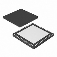
IC, 16BIT MCU, PIC24F, 32MHZ, QFN-64
Manufacturer
Microchip Technology
Series
PIC® 24Fr
Datasheets
1.PIC24FJ128GA008-IPT.pdf
(12 pages)
2.PIC24FJ128GA106-IPT.pdf
(14 pages)
3.PIC24FJ128GA106-IPT.pdf
(330 pages)
4.PIC24FJ128GA106-IPT.pdf
(52 pages)
5.PIC24FJ256GA106-IPT.pdf
(59 pages)
6.PIC24FJ128GB110-IPF.pdf
(292 pages)
Specifications of PIC24FJ256GA106-I/MR
Controller Family/series
PIC24
No. Of I/o's
53
Ram Memory Size
16KB
Cpu Speed
32MHz
No. Of Timers
5
Core Size
16 Bit
Program Memory Size
256KB
Peripherals
ADC, Comparator, PWM, RTC, Timer
Core Processor
PIC
Speed
32MHz
Connectivity
I²C, PMP, SPI, UART/USART
Number Of I /o
53
Program Memory Type
FLASH
Ram Size
16K x 8
Voltage - Supply (vcc/vdd)
2 V ~ 3.6 V
Data Converters
A/D 16x10b
Oscillator Type
Internal
Operating Temperature
-40°C ~ 85°C
Package / Case
64-VFQFN, Exposed Pad
Processor Series
PIC24FJ
Core
PIC
Data Bus Width
16 bit
Data Ram Size
16 KB
Interface Type
I2C, SPI, UART
Maximum Clock Frequency
32 MHz
Number Of Programmable I/os
52
Number Of Timers
5
Maximum Operating Temperature
+ 85 C
Mounting Style
SMD/SMT
3rd Party Development Tools
52713-733, 52714-737, 53276-922, EWDSPIC
Development Tools By Supplier
PG164130, DV164035, DV244005, DV164005, PG164120, DM240001, DM240011
Minimum Operating Temperature
- 40 C
On-chip Adc
10 bit, 16 Channel
Lead Free Status / RoHS Status
Lead free / RoHS Compliant
For Use With
876-1004 - PIC24 BREAKOUT BOARD
Eeprom Size
-
Lead Free Status / Rohs Status
Details


PIC24FJXXXDA1/DA2/GB2/GA3
3.2.2
The REGOUT control code allows for data to be
extracted from the device in ICSP mode. It is used to
clock the contents of the VISI register, out of the device,
over the PGEDx pin. After the REGOUT control code is
received, the CPU is held Idle for 8 cycles. After these
8 cycles, an additional 16 cycles are required to clock the
data out (see
The REGOUT code is unique because the PGEDx pin
is an input when the control code is transmitted to the
device. However, after the control code is processed,
the PGEDx pin becomes an output as the VISI register
is shifted out.
FIGURE 3-3:
DS39970B-page 16
PGECx
PGEDx
Fetch REGOUT Control Code
Execute Previous Instruction, CPU Held in Idle
1
REGOUT SERIAL INSTRUCTION
EXECUTION
1
Figure
0
2
PGEDx = Input
0
3
3-3).
0
REGOUT SERIAL EXECUTION
4
P4
1
2
7
8
P5
LSb
1
1
2
2
3
3
4
Shift Out VISI Register<15:0>
4
5
PGEDx = Output
...
Note 1: After the contents of VISI are shifted out,
6
10
11
2: Data changes on the falling edge and
11
12
the
devices maintain PGEDx as an output
until the first rising edge of the next clock
is received.
latches on the rising edge of PGECx. For
all
Significant bit (LSb) is transmitted first.
12
13
13
14
data
14
PIC24FJXXXDA1/DA2/GB2/GA3
15 16
MSb
2010 Microchip Technology Inc.
transmissions,
P4A
0
No Execution Takes Place,
Fetch Next Control Code
1
PGEDx = Input
0
2
0
3
the
0
4
Least
Related parts for PIC24FJ256GA106-I/MR
Image
Part Number
Description
Manufacturer
Datasheet
Request
R

Part Number:
Description:
Manufacturer:
Microchip Technology Inc.
Datasheet:
Part Number:
Description:
Manufacturer:
Microchip Technology Inc.
Datasheet:
Part Number:
Description:
Manufacturer:
Microchip Technology Inc.
Datasheet:
Part Number:
Description:
Manufacturer:
Microchip Technology Inc.
Datasheet:
Part Number:
Description:
Manufacturer:
Microchip Technology Inc.
Datasheet:
Part Number:
Description:
Manufacturer:
Microchip Technology Inc.
Datasheet:
Part Number:
Description:
Manufacturer:
Microchip Technology Inc.
Datasheet:
Part Number:
Description:
Manufacturer:
Microchip Technology Inc.
Datasheet: