PIC24FJ256GA106-I/MR Microchip Technology, PIC24FJ256GA106-I/MR Datasheet - Page 54
PIC24FJ256GA106-I/MR
Manufacturer Part Number
PIC24FJ256GA106-I/MR
Description
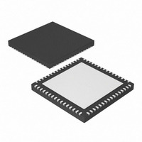
IC, 16BIT MCU, PIC24F, 32MHZ, QFN-64
Manufacturer
Microchip Technology
Series
PIC® 24Fr
Datasheets
1.PIC24FJ128GA008-IPT.pdf
(12 pages)
2.PIC24FJ128GA106-IPT.pdf
(14 pages)
3.PIC24FJ128GA106-IPT.pdf
(330 pages)
4.PIC24FJ128GA106-IPT.pdf
(52 pages)
5.PIC24FJ256GA106-IPT.pdf
(59 pages)
6.PIC24FJ128GB110-IPF.pdf
(292 pages)
Specifications of PIC24FJ256GA106-I/MR
Controller Family/series
PIC24
No. Of I/o's
53
Ram Memory Size
16KB
Cpu Speed
32MHz
No. Of Timers
5
Core Size
16 Bit
Program Memory Size
256KB
Peripherals
ADC, Comparator, PWM, RTC, Timer
Core Processor
PIC
Speed
32MHz
Connectivity
I²C, PMP, SPI, UART/USART
Number Of I /o
53
Program Memory Type
FLASH
Ram Size
16K x 8
Voltage - Supply (vcc/vdd)
2 V ~ 3.6 V
Data Converters
A/D 16x10b
Oscillator Type
Internal
Operating Temperature
-40°C ~ 85°C
Package / Case
64-VFQFN, Exposed Pad
Processor Series
PIC24FJ
Core
PIC
Data Bus Width
16 bit
Data Ram Size
16 KB
Interface Type
I2C, SPI, UART
Maximum Clock Frequency
32 MHz
Number Of Programmable I/os
52
Number Of Timers
5
Maximum Operating Temperature
+ 85 C
Mounting Style
SMD/SMT
3rd Party Development Tools
52713-733, 52714-737, 53276-922, EWDSPIC
Development Tools By Supplier
PG164130, DV164035, DV244005, DV164005, PG164120, DM240001, DM240011
Minimum Operating Temperature
- 40 C
On-chip Adc
10 bit, 16 Channel
Lead Free Status / RoHS Status
Lead free / RoHS Compliant
For Use With
876-1004 - PIC24 BREAKOUT BOARD
Eeprom Size
-
Lead Free Status / Rohs Status
Details


PIC24FJXXXDA1/DA2/GB2/GA3
6.0
6.1
The Device ID region of memory can be used to
determine
information about the chip. The Device ID region is
2 x 16 bits and it can be read using the READC
command. This region of memory is read-only and can
also be read when code protection is enabled.
Table 6-1
Table 6-2
lists and describes the bit field of each register.
TABLE 6-2:
TABLE 6-3:
6.2
Checksums for the PIC24FJXXXDA1/DA2/GB2/GA3
families are 16 bits in size. The checksum is calculated
by summing the following:
• Contents of code memory locations
• Contents of Configuration registers
DS39970B-page 54
FF0000h
FF0002h
FAMID<7:0>
DEV<7:0>
REV<3:0>
Address
Bit Field
DEVICE DETAILS
Device ID
Checksum Computation
provides the Device ID registers and
provides the Device ID for each device,
mask,
DEVID
DEVREV
PIC24FJXXXDA1/DA2/GB2/GA3 DEVICE ID REGISTERS
DEVICE ID BIT DESCRIPTIONS
Name
variant
DEVID
DEVID
DEVREV
Register
15
and
14
manufacturing
13
Table 6-3
FAMID<7:0>
Encodes the family ID of the device.
Encodes the individual ID of the device.
Encodes the sequential (numerical) revision identifier of the device.
12
11
10
—
calculate the checksum for each device. All memory
TABLE 6-1:
Table 6-4
locations are summed, one byte at a time, using only
their native data size. Especially, Configuration registers
are summed by adding the lower two bytes of these
locations (the upper byte is ignored), while code memory
is summed by adding all three bytes of code memory.
PIC24FJ128DA106
PIC24FJ256DA106
PIC24FJ128DA110
PIC24FJ256DA110
PIC24FJ128DA206
PIC24FJ256DA206
PIC24FJ128DA210
PIC24FJ256DA210
PIC24FJ64GA306
PIC24FJ64GA308
PIC24FJ64GA310
PIC24FJ128GA306
PIC24FJ128GA308
PIC24FJ128GA310
PIC24FJ128GB206
PIC24FJ256GB206
PIC24FJ128GB210
PIC24FJ256GB210
9
8
Bit
Device
lists the devices and describes how to
Description
7
DEVICE IDs
6
5
2010 Microchip Technology Inc.
DEV<7:0>
4
3
DEVID
46CA
410D
410B
410F
410C
410A
410E
46C0
46C4
46C8
46C2
46C6
REV<3:0>
4109
4108
4100
4104
4102
4106
2
1
0
Related parts for PIC24FJ256GA106-I/MR
Image
Part Number
Description
Manufacturer
Datasheet
Request
R

Part Number:
Description:
Manufacturer:
Microchip Technology Inc.
Datasheet:
Part Number:
Description:
Manufacturer:
Microchip Technology Inc.
Datasheet:
Part Number:
Description:
Manufacturer:
Microchip Technology Inc.
Datasheet:
Part Number:
Description:
Manufacturer:
Microchip Technology Inc.
Datasheet:
Part Number:
Description:
Manufacturer:
Microchip Technology Inc.
Datasheet:
Part Number:
Description:
Manufacturer:
Microchip Technology Inc.
Datasheet:
Part Number:
Description:
Manufacturer:
Microchip Technology Inc.
Datasheet:
Part Number:
Description:
Manufacturer:
Microchip Technology Inc.
Datasheet: