PIC24FJ256GA106-I/MR Microchip Technology, PIC24FJ256GA106-I/MR Datasheet - Page 34
PIC24FJ256GA106-I/MR
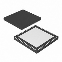
Manufacturer Part Number
PIC24FJ256GA106-I/MR
Description
IC, 16BIT MCU, PIC24F, 32MHZ, QFN-64
Manufacturer
Microchip Technology
Series
PIC® 24Fr
Datasheets
1.PIC24FJ128GA008-IPT.pdf
(12 pages)
2.PIC24FJ128GA106-IPT.pdf
(14 pages)
3.PIC24FJ128GA106-IPT.pdf
(330 pages)
4.PIC24FJ128GA106-IPT.pdf
(52 pages)
5.PIC24FJ256GA106-IPT.pdf
(59 pages)
6.PIC24FJ128GB110-IPF.pdf
(292 pages)
Specifications of PIC24FJ256GA106-I/MR
Controller Family/series
PIC24
No. Of I/o's
53
Ram Memory Size
16KB
Cpu Speed
32MHz
No. Of Timers
5
Core Size
16 Bit
Program Memory Size
256KB
Peripherals
ADC, Comparator, PWM, RTC, Timer
Core Processor
PIC
Speed
32MHz
Connectivity
I²C, PMP, SPI, UART/USART
Number Of I /o
53
Program Memory Type
FLASH
Ram Size
16K x 8
Voltage - Supply (vcc/vdd)
2 V ~ 3.6 V
Data Converters
A/D 16x10b
Oscillator Type
Internal
Operating Temperature
-40°C ~ 85°C
Package / Case
64-VFQFN, Exposed Pad
Processor Series
PIC24FJ
Core
PIC
Data Bus Width
16 bit
Data Ram Size
16 KB
Interface Type
I2C, SPI, UART
Maximum Clock Frequency
32 MHz
Number Of Programmable I/os
52
Number Of Timers
5
Maximum Operating Temperature
+ 85 C
Mounting Style
SMD/SMT
3rd Party Development Tools
52713-733, 52714-737, 53276-922, EWDSPIC
Development Tools By Supplier
PG164130, DV164035, DV244005, DV164005, PG164120, DM240001, DM240011
Minimum Operating Temperature
- 40 C
On-chip Adc
10 bit, 16 Channel
Lead Free Status / RoHS Status
Lead free / RoHS Compliant
For Use With
876-1004 - PIC24 BREAKOUT BOARD
Eeprom Size
-
Lead Free Status / Rohs Status
Details


PIC24FJXXXDA1/DA2/GB2/GA3
TABLE 4-2:
DS39970B-page 34
SOSCSEL<1:0>
WDTPS<3:0>
WINDIS
WPCFG
WPDIS
WPEND
WPFP<7:0>
WUTSEL<1:0>
Note 1:
2:
3:
Bit Field
Bits<23-16> should be programmed to a value of 0x00 to ensure that accidental program execution of any
of the Configuration Words would be interpreted as a NOP opcode.
The JTAGEN bit can be modified using only In-Circuit Serial Programming™ (ICSP™).
Irrespective of the WPCFG status, if WPEND = 1 or if WPFP corresponds to the Configuration Words
page, the Configuration Words page will be protected
PIC24FJXXXDA1/DA2/GB2 CONFIGURATION BITS DESCRIPTION (CONTINUED)
CW3<11:10> Voltage Regulator Standby Mode Wake-up Time Select bits
Register
CW3<9:8>
CW1<3:0>
CW3<7:0>
CW3<14>
CW3<13>
CW3<15>
CW1<6>
(1)
SOSC Selection Configuration bits
11 = Secondary oscillator in Default (high drive strength) Oscillator mode
10 = Reserved; do not use
01 = Secondary oscillator in Low-Power (low drive strength) Oscillator
00 = External clock (SCLKI) or Digital I/O mode
Watchdog Timer Postscaler bits
1111 = 1:32,768
1110 = 1:16,384
0001 = 1:2
0000 = 1:1
Windowed WDT bit
1 = Standard Watchdog Timer is enabled
0 = Windowed Watchdog Timer is enabled; FWDTEN must be ‘1’
Configuration Word Code Page Write Protection Select bit
1 = Last page (at the top of program memory) and Flash Configuration
0 = Last page and Flash Configuration Words are write-protected
Segment Write Protection Disable bit
1 = Segmented code protection is disabled
0 = Segmented code protection is enabled; protected segment defined
Segment Write Protection End Page Select bit
1 = Protected code segment upper boundary is at the last page of program
0 = Protected code segment lower boundary is at the bottom of program
Write-Protected Code Segment Boundary Page bits
Designate the 512-instruction page that is the boundary of the protected
code segment, starting with Page 0 at the bottom of program memory.
If WPEND = 1:
First address of designated code page is the lower boundary of the segment;
the last implemented page will be the last write-protected page.
If WPEND = 0:
Last address of designated code page is the upper boundary of
the segment.
11 = Default regulator start-up time is used
01 = Fast regulator start-up time is used
x0 = Reserved; do not use
Words are not write-protected
provided, WPDIS = 0
by the WPEND, WPCFG and WPFPx Configuration bits
memory; lower boundary is the code page specified by WPFP<7:0>
memory (000000h); upper boundary is the code page specified by
WPFP<7:0>
mode
.
.
.
Description
(3)
2010 Microchip Technology Inc.
Related parts for PIC24FJ256GA106-I/MR
Image
Part Number
Description
Manufacturer
Datasheet
Request
R

Part Number:
Description:
Manufacturer:
Microchip Technology Inc.
Datasheet:
Part Number:
Description:
Manufacturer:
Microchip Technology Inc.
Datasheet:
Part Number:
Description:
Manufacturer:
Microchip Technology Inc.
Datasheet:
Part Number:
Description:
Manufacturer:
Microchip Technology Inc.
Datasheet:
Part Number:
Description:
Manufacturer:
Microchip Technology Inc.
Datasheet:
Part Number:
Description:
Manufacturer:
Microchip Technology Inc.
Datasheet:
Part Number:
Description:
Manufacturer:
Microchip Technology Inc.
Datasheet:
Part Number:
Description:
Manufacturer:
Microchip Technology Inc.
Datasheet: