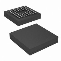
CY7C68053-56BAXIT Cypress Semiconductor Corp, CY7C68053-56BAXIT Datasheet - Page 30

CY7C68053-56BAXIT
Manufacturer Part Number
CY7C68053-56BAXIT
Description
CY7C68053-56BAXIT
Manufacturer
Cypress Semiconductor Corp
Series
MoBL-USB™r
Datasheet
1.CY7C68053-56BAXI.pdf
(42 pages)
Specifications of CY7C68053-56BAXIT
Applications
USB Microcontroller
Core Processor
8051
Program Memory Type
ROMless
Controller Series
CY7C680xx
Ram Size
16K x 8
Interface
I²C, USB
Number Of I /o
56
Voltage - Supply
1.71 V ~ 1.89 V
Operating Temperature
-40°C ~ 85°C
Mounting Type
Surface Mount
Package / Case
56-VFBGA
Processor Series
CY7C68xx
Core
8051
Data Bus Width
8 bit
Data Ram Size
16 KB
Interface Type
I2C
Maximum Clock Frequency
48 MHz
Number Of Programmable I/os
24
Maximum Operating Temperature
+ 85 C
Mounting Style
SMD/SMT
Minimum Operating Temperature
- 40 C
Lead Free Status / RoHS Status
Lead free / RoHS Compliant
For Use With
CY3687 - KIT DEV MOBL-USB FX2LP18
Lead Free Status / Rohs Status
Details
Available stocks
Company
Part Number
Manufacturer
Quantity
Price
Company:
Part Number:
CY7C68053-56BAXIT
Manufacturer:
Cypress Semiconductor Corp
Quantity:
10 000
There is no specific timing requirement to be met for asserting
the PKTEND pin with regards to asserting SLWR. PKTEND can
be asserted with the last data value clocked into the FIFOs or
thereafter. The only consideration is that the setup time t
the hold time t
Although there are no specific timing requirements for the
PKTEND assertion, there is a specific corner case condition that
needs attention while using the PKTEND to commit a one
byte/word packet. There is an additional timing requirement to be
met when the FIFO is configured to operate in auto mode and
you want to send two packets back to back: a full packet (full
defined as the number of bytes in the FIFO meeting the level set
in AUTOINLEN register) committed automatically followed by a
short one byte/word packet committed manually using the
PKTEND pin. In this scenario, make sure to assert PKTEND at
9.8 Slave FIFO Asynchronous Packet End Strobe
Table 20. Slave FIFO Asynchronous Packet End Strobe Parameters
Document # 001-06120 Rev *J
t
t
t
PEpwl
PWpwh
XFLG
PKTEND
FIFOADR
DATA
IFCLK
SLWR
Parameter
PEH
must be met.
Figure 14. Slave FIFO Synchronous Write Sequence and Timing Diagram
PKTEND pulse width LOW
PKTEND pulse width HIGH
PKTEND to FLAGS output propagation delay
Figure 15. Slave FIFO Asynchronous Packet End Strobe Timing Diagram
t
SFA
t
IFCLK
>= t
t
SFD
PKTEND
SWR
X-4
FLAGS
t
FDH
Description
t
SFD
X-3
t
FDH
SPE
and
t
SFD
X-2
t
PEpwl
t
XFLG
t
FDH
least one clock cycle after the rising edge that caused the last
byte/word to be clocked into the previous auto committed packet.
Figure 14
register is set to when the IN endpoint is configured to be in auto
mode.
Figure 14
The first packet is committed automatically when the number of
bytes in the FIFO reaches X (value set in AUTOINLEN register)
and the second one byte/word short packet is committed
manually using PKTEND. Note that there is at least one IFCLK
cycle timing between the assertion of PKTEND and clocking of
the last byte of the previous packet (causing the packet to be
committed automatically). Failing to adhere to this timing, results
in the FX2LP18 failing to send the one byte/word short packet.
[19]
t
SFD
X-1
t
shows this scenario. X is the value the AUTOINLEN
shows a scenario where two packets are committed.
PEpwh
t
FDH
Min
50
50
t
SFD
X
t
FDH
At least one IFCLK cycle
[16]
Max
115
t
SFD
[16]
1
>= t
t
FDH
WRH
CY7C68053
t
t
FAH
SPE
Unit
ns
ns
ns
Page 30 of 42
t
PEH
[+] Feedback


